PayPal info needed
Hi all,
I've received 8 PayPal accounts and shipping addresses so far.
Remaining partecipants are asked to PM me PayPal account and shipping addresses:
Hi all,
I've received 8 PayPal accounts and shipping addresses so far.
Remaining partecipants are asked to PM me PayPal account and shipping addresses:
- Randytsuch
- alex70ita
- billo44
- TjongKristian
- arthur
- Pmeade
- Badrisuper
Have Wima, or any other manufacturer, replaced the FKI ?
How do MKI compare?
Evox SFR, if it's still available - most probably magnetic leads.
Never laid my hands on both MKI2 and FKI2 in the same value, so no idea. But FKI2 sounded comparable to FKP2, IIRC.
One of the Italians withdrew because he fear to not be able to solder components... 😱
The GB goes on anyway on same conditions, I'll take his boards.
If further defections will appear production will be moved from Italy to China (PCBCart), so that even with smaller numbers price will be the same or lower.
The GB goes on anyway on same conditions, I'll take his boards.
If further defections will appear production will be moved from Italy to China (PCBCart), so that even with smaller numbers price will be the same or lower.
If further defections will appear production will be moved from Italy to China (PCBCart), so that even with smaller numbers price will be the same or lower.
Check out PCB Power (India) Ltd.:
Welcome to PCBPower.com
They accept Gerber/Excellon files, and Eagle output works perfectly. The finish is superb, and they do Immersion Gold and Silver (optional). You need to register and be validated to place an order, but almost everything else, including price estimations, can be done online for free.
I estimate that you'll save about 50% in prototype quantities (up to 5-6 PCBs) and maybe 60-80% in slightly larger volumes over EU vendors, even after taking shipping into account. This is because they can do pooled services, where your PCBs will be placed in vacant spaces on larger production panels, thus allowing large discounts. Sometimes, you'll get an upgraded finish for free, like Immersion Gold, in pooled services - if there's a panel with that finish that has vacant area.
If you can't register or set up an account for any reason, I can order it on my account - but you'll need to send the Gerbers/Excellons to me, if you're OK with it. My credit-limit with them is a bit low, at about $200, but it goes a long way in pooled services, enough for 20-40 boards, maybe more if you're willing to accept 25-30 day lead times.
Last edited:
Check out PCB Power (India) Ltd.:
(...)
If you can't register or set up an account for any reason, I can order it on my account - but you'll need to send the Gerbers/Excellons to me, if you're OK with it.
Hi Siva,
it's very kind, thanks.
I'm emailing you but I'll probably stick with PCBCart.
Dario
One out, one in: 🙂
- ClaveFremen x 2 (IT)
- Suburra x2 (IT)
- SoIL4x4 (US)
- Bmcbob (US)
- Randytsuch (US)
- MrSavage 2x (US)
- b.veneri (IT)
- StefanoSan73 (IT)
- diymax62 (IT)
- billo44 (UK/JP?)
- TjongKristian (ID)
- arthur x 2 (N/A)
- PMeade (US)
- Badrisuper (IN)
- lehmanhill x2 (US)
- KSTR (DE)
- Randytsuch
- MrSavage
- billo44
- TjongKristian
- arthur
- Pmeade
- Badrisuper
Adding a parallel load to the power supply
I'm thinking about using one pair of boards for speakers that get a balanced input from the pre-amp. That means I need to power an INA134 balanced line receiver at the amp. It is a small unity gain opamp that should only add 3 ma current to the load.
I don't have much experience with a CCS power supply. Would I do anything different to the power supply build if I wanted to parallel the INA134 from the FE on board power supply?
I don't have much experience with a CCS power supply. Would I do anything different to the power supply build if I wanted to parallel the INA134 from the FE on board power supply?
I think you can use the regulator as is without problems but it's posiible that you'll need to mount regulator's output capacitors (C102, C202).
Ideally I would also lower a bit the current setting resistors, say 47R just to have a bit more margin, but sadly 47R MP915s are not available from Mouser.
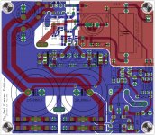
Release Candidate PCBs and schematic
I've attached the first version of the Release Candidate PCBs layout, schematic and preliminary BOM.
Rev A/B compatibility has been removed.
Main changes from beta boards:
Comments and suggestions are welcome 🙂
I've attached the first version of the Release Candidate PCBs layout, schematic and preliminary BOM.
Rev A/B compatibility has been removed.
Main changes from beta boards:
- R12 and R7 are now SMD to use the superb Susumu
- R13 is a Caddock MK132 (the position fits both Caddocks and 1/2W resistors)
- All Caddock MK132 positions can fit less expensive 1/2W parts
- LM318's compensation networks now use SMD parts only
- All boxed capacitors have indicated outer foil (direction)
- All signal resistors have indicated direction.
- C13 is now Audyn True Copper or Vishay/Sprague V-735-P
- Big smoothing caps now can be 35mm
- All faston positions have an integrated wirepad
- LM318 PS now uses LM317s for both polarities (better rejection)
- Thermals have been reduced by 20% for easier soldering
- Clearance between pads and ground planes has been increased from 12 to 16 mils for easier manifacturing.
- All holes are aligned to a 10 mils grid for easier manifacturing.
Comments and suggestions are welcome 🙂
Attachments
Last edited:
I've attached the first version of the Release Candidate PCBs layout, schematic and preliminary BOM.
Comments and suggestions are welcome 🙂
Hi Dario - looks nice! I do have some suggestions (which may look a bit radical, but are actually fairly simple to implement - maybe 1-2 hours work at most).
1) Make both ground planes on the same layer (bottom).
2) Shift all the tracks in the small-signal area, as well as (almost) all the SMD outlines, to the top layer. Only a few components like C7 and C32 have to be shifted slightly to prevent mechanical interference with the SMD components.
3) A few tracks (1 or 2) in the small-signal area (which cross tracks on the other layer) go to the bottom layer.
What it achieves is that you can use a single silkscreen on the component side only, which allows the use of high-volume PCB processes which may reduce costs by half. When two silkscreens are used, some processes (including PCBPower's Verified flow) cannot be used, and a more expensive flow like Verified Plus has to be used.
Hi Dario - looks nice! I do have some suggestions (which may look a bit radical, but are actually fairly simple to implement - maybe 1-2 hours work at most).
(...)
What it achieves is that you can use a single silkscreen on the component side only, which allows the use of high-volume PCB processes which may reduce costs by half.
Hi Siva,
thanks 🙂
Using standard production processes PCBCart difference between two side silkscreen and one side only is 1.2€, PCB-Proto (the Italian manifacturer) carries 18€.
It translates in a difference of 0.45€ per PCB (0.03%).
Not worth the effort... 😉
In addition having SMD components on the upper side has a major drawback:
If you need to replace for whatever reason a SMD part (like I've had to do to replace a defective LM318) you need clearance and you have pratically none if you mount SMDs on the upper side.
Google folder just updated
I've updated Release Candidate Google folder with latest schematic, PCB and Eagle files.
I've updated Release Candidate Google folder with latest schematic, PCB and Eagle files.
My 2cents, 90% of all the problems I have had with all my LM3886 (other than not paying attention to detail) are due to the loss of vias (metal sleeve passing top to bottom of PCB) on thru-hole and/or the loss of a pad due to excess heat.
Unless a builder uses sockets this problem may be somewhat significant for tweakers. IMHO, the elimination of as many as possible of those via spots would be beneficial.
The solution may just be in the manufacturing process/specs - but I for one would pay a few dollars more for a board crafted to lessen the possibility of thru-hole gotchas.
Last edited:
Unless a builder uses sockets this problem may be somewhat significant for tweakers. IMHO, the elimination of as many as possible of those via spots would be beneficial.
Mmh, this problem is common on all PCBs in general, even in single layer ones it's possibile to destroy the PCB...
I can't see how to improve it in layout... do you have some specific ideas on places to be revised?
The solution may just be in manufacturing process/specs - and I for one would pay a few dollars more for a board crafted to lessen the possibility of thru-hole gotchas.
This is already in project specifications (2 Oz copper) and depends also on the quality of materials used.
The use of 2 Oz copper (needed to offer more current capability to traces) also results in a PCB that is more resistant to misuse.
BTW the best way to avoid such problems is the use of proper tools like a desoldering station...😉
Agreed on all points. However, many amp builder may not have, or don't want to, or can't invest in some of the better tools. My comments were not directed toward any specific PCB (the beta FEs are in fact some of the best I have worked with) but just reporting my general frustration with what I see as the weakest area in DIYing.
I am not technically savvy enough to propose specific item recommendations. I'm only attempting to express a concern to all who are considering board design and component placement, particularly with the novice builder in mind.
I am not technically savvy enough to propose specific item recommendations. I'm only attempting to express a concern to all who are considering board design and component placement, particularly with the novice builder in mind.
Last edited:
Dario, speaking of soldering, I can't find the Chip Quick alloy at Mouser. Could you please re-post the item number.
Thanks.
Thanks.
Dario, speaking of soldering, I can't find the Chip Quick alloy at Mouser. Could you please re-post the item number.
Desoldering alloy startert kit (910-SMD1NL)
But if you already have the tacky flux (910-SMD291NL) you may find more convenient the desoldering alloy alone (910-SMD4.5NL).

- Status
- Not open for further replies.
- Home
- Amplifiers
- Chip Amps
- My_Ref Fremen Edition - Beta build/Fine tuning