Member
Joined 2009
Paid Member
Perhaps in addition to the simple zener we should consider the TL431 - essentially an adjustable zener ? I know Hugh is a fan of these 3 legged critters.
I agree with everything you said Hugh, I'll see how I can handle the BOM before I send you a email.
I think the powersupply design will be off limits for me.
Hopefully I'll get a little more progress on board.
I think the powersupply design will be off limits for me.
Hopefully I'll get a little more progress on board.
Kurt,
Looks terrific.
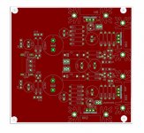
Can you send me a composite, showing all tracks and component designations, maybe with the schematic and matching designations that you are using?
I will then check it.....
Thanks mate, great job,
Hugh
Looks terrific.
Can you send me a composite, showing all tracks and component designations, maybe with the schematic and matching designations that you are using?
I will then check it.....
Thanks mate, great job,
Hugh
Since I can't really send attachments though PM's so I'll leave the schematic I was using (the schematic and the boardlayout is linked, changes that happen to the schematic happen on the board). I'll make a later identical layout with values, unless someone else would like to.
Currently, the board layout doesn't have any traces, I hid all the lines that had gone to 0V or V+/V-. I need to adjust the layout of the PS section before I do any routing.
Currently, the board layout doesn't have any traces, I hid all the lines that had gone to 0V or V+/V-. I need to adjust the layout of the PS section before I do any routing.
Attachments
I think this should be a small milestone, Just need to rename a bunch of parts, tweak one or two traces and create a professional looking schematic, could anyone recommend a nice program for creating nice looking schematics?
I feel like I've finally accomplished something significant
I'd like to know if anyone would be interested in distributing? or who might be able to organize the GB.
I feel like I've finally accomplished something significant
I'd like to know if anyone would be interested in distributing? or who might be able to organize the GB.
Attachments
I'm very impressed, KofA. This is something I've tried several times to do and have always struggled. It looks fantastic.
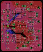
Avoid angles less than 90 degrees.
If you start with a schematics then you have a big help to get a correct pcb since you have a connection between those two.
If you start with a schematics then you have a big help to get a correct pcb since you have a connection between those two.
P-A,
Why do you avoid angles less than 90 degrees? Would 45 degrees be OK? My boards use lots of small angles, and curves, too, am I doing it all wrong?
BTW, I'd argue with your 'yellow electrons'. It actually depends how fast they are going, they change color due to Doppler shift. Observing their color is tricky however; concentrate hard, and you become very uncertain. Treat them casually, and they can strike your eye, causing serious damage. Have you any color electrographs? (no cloud chamber trails, please.)
Ciao,
Hugh
Hugh, sharp angles creates acid traps which can be critical if the trace is thin but in this particular layout it's not a problem more than it looks not very professional. The sharp angle is a T-crossing at the left.
Knight, I'll suggest tjat most if the tracks are located at the component side since à whole groundplane is desired. Normally I had put the groundplane at the component side (looks nicer) but since you have heatsinks it's better with the groundplane on the solderside.
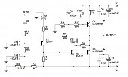
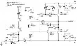
The connection between C1V/C2V and D1V/D2V is unnessary. The schematic symbol is also wrong since the parts are LED's
I also once saw some pictures, I think it had to do with early capacitors involving glass jars and plates. Anyway the pictures showed the radiation that eminates from the plates, and it was particularly concentrated around edges and the sharp corners, not so much over the flat surface area though....
I believe I can remove the ground plane underneath the heat sinks...Knight, I'll suggest tjat most if the tracks are located at the component side since à whole groundplane is desired. Normally I had put the groundplane at the component side (looks nicer) but since you have heatsinks it's better with the groundplane on the solderside.
Does anyone know how much Q3 and Q4 dissipate?
Any part ending with a V is a optional component for people who want to use a virtual ground and a duel rail powersupply, The correct LED's are there, check post #1085... That's the current schematic I'm using (which is linked to the board layout)The connection between C1V/C2V and D1V/D2V is unnessary. The schematic symbol is also wrong since the parts are LED's
A couple more things that I should note, the headphone out for both channels is paired with a test point, they should not be used for headphone ground. The main star ground via should be used if a TRS style jack is used. This should allow me to make the ground wires a little less messy.
Last edited:
This is the schematic that will be used for a building aid... Just needs a little added ownership
and the BOM is almost done, just needs some more parts and final touches.
Kurt,
Please excuse my breaking in to your post!!
R3 would be 820R and a 500R pot in series.... this permits trimming the output offset to zero, very, very important for a headphone amp.
Hugh
and the BOM is almost done, just needs some more parts and final touches.
Kurt,
Please excuse my breaking in to your post!!
R3 would be 820R and a 500R pot in series.... this permits trimming the output offset to zero, very, very important for a headphone amp.
Hugh
Attachments
Last edited by a moderator:
Oh, that scared me! I didn't write that! 😛
Ok, I'll make the changes to the board layout and schematic, a DC trim is pretty significant...
Current state of BOM:
https://spreadsheets.google.com/ccc...hMlNwbWhFMDg2RlE&hl=en&authkey=CKH76_oB#gid=0
Ok, I'll make the changes to the board layout and schematic, a DC trim is pretty significant...
Current state of BOM:
https://spreadsheets.google.com/ccc...hMlNwbWhFMDg2RlE&hl=en&authkey=CKH76_oB#gid=0
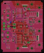
I should also have the most current PCB, there's still one or two things that need to be done, but other then that; how does it look?
And added the fine schematic
And added the fine schematic
Attachments
Last edited:
Kurt,
Looks very good, but as commented privately I will check it out in detail tomorrow.
Again, my thanks,
Hugh
Looks very good, but as commented privately I will check it out in detail tomorrow.
Again, my thanks,
Hugh
One important thing is forgotten. The output should have a 120 ohm resistor in series. This will create the standard output impedance eventhough I prefer to be able to short this resistor. You can check out my QRV09 design for inspiration.
The gain is nearly 20 dB which is too much in many cases. The design should be tested for gains down to 6 dB.
The gain is nearly 20 dB which is too much in many cases. The design should be tested for gains down to 6 dB.
Last edited:
How many sets of 'phones are designed to the 120ohm output impedance standard? 99% of 'phones amps I've seen have touted their low output impedance as a feature.
- Home
- More Vendors...
- AKSA
- Aspen Headphone Amp