Transistor choice
Hi OS,
I will etch the PCB for GX this weekend.
I intend to use the 2SA1930 & 2SC5171 as driver (Q96 & Q97) on the PB120. I have 6 pairs of those and the spec looks better than the A1837/C4793 pair.
I only bought two pairs of A1360/C3423 for VAS on GX1.2, I measured their Hfe:
A1360 #1 - Hfe=213 as Q9?
A1360 #2 - Hfe=155 as Q10?
C3423 #1 - Hfe=167 as Q12?
C3423 #2 - Hfe=145 as Q11?
Should I use the higher gain parts out of the two pairs as Q9 & Q12?
Can you please give me a recommendation of the resistors value for GX for 42V-DC rails?
Cheers, Stanley
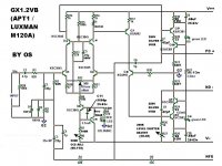
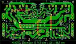
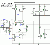
GX is totally debugged now. Schematic ,overview , and BOM updated. SNG , the below values and the updated Zip in my website"mongel" folder will work nicely at 42-0-42V ... this is the test supply in the "mongrel lab", BTW (45-0-45VDC).
A quick adjustment of "CCS ADJ." for 1.25-1.3ma per tail (Q1-2) will be all that is required. On the topic of those adjustments (R6/R12/R27) , see below.
R6 = CCS adj.This adjustment controls both the tail currents and subsequently the VAS standing current. You can either use my recommended values below (GX1.2VB_complete.Zip) or experiment with the VAS Re's (R19/25-68R) and the
"magic resistors" (R20/24 - 33R). adjustment of the CCS can re-establish the 6.5ma standing current of the VAS even with different resistor values. I have mine set at 95R which equates to 1.27ma in both Q1 and 2.
R27 is the "level shifter adjust" . You adjust this to get the best balance at the input pair (lowest offset). On first try my module had 14mv offset with this adjustment at 40R.
R12 is the main "offset adj." . after doing the first 2 above I was able to trim the offset to under 1mv with about 2 turns on the 25-turn 500R trimmer.
When looking at a scope with a 500hz test signal , you will see the waveform superimpose (match) between the emitters of Q1/2 when using a dual trace scope. Again ,this happened with 35-45R at R27's adjustment. I also tried different currents for the input pair , everything ran well from 80-115R (1.6 - 1ma) , at 1ma and below , a slight harshness occurred. At 1.6 and above , the VAS ran too hot (10ma+).
Below is the new schema ... not changed much but concise. It is now officially approved as hardy, safe and VERY good sounding.
OS
Attachments
Hi OS,
Is this sounding better than your Mongrel GX?
Thanks,
Mark
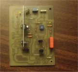
That is the mongrel GX !! 🙂
Hi Os,
It appears that the top mirror file is actually not mirrored in your GX folder.
I plan on attempting my first diy pcb this weekend.
Pete.
It appears that the top mirror file is actually not mirrored in your GX folder.
I plan on attempting my first diy pcb this weekend.
Pete.
GX is totally debugged now. Schematic ,overview , and BOM updated. SNG , the below values and the updated Zip in my website"mongel" folder will work nicely at 42-0-42V ... this is the test supply in the "mongrel lab", BTW (45-0-45VDC).
Below is the new schema ... not changed much but concise. It is now officially approved as hardy, safe and VERY good sounding.
OS
Hi OS,
Thanks for the update, I will follow your setup procedure.
Cheers, Stanley
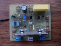
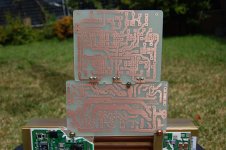
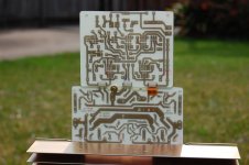
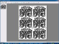
PCB file for GX1.2 VB
Hi Pete,
I have etched the PCB for GX1.2VB. I used MS Paint to open GX1.2VB_PCB.jpg and just print at 100% (no scaling & no need to select mirror in printer setup).
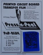
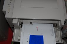
I have attached two picture here. BTW, I used Press-n-Peel blue film & I get good toner transfer every time.
Cheers, Stanley
Hi Os,
It appears that the top mirror file is actually not mirrored in your GX folder.
I plan on attempting my first diy pcb this weekend.
Pete.
Hi Pete,
I have etched the PCB for GX1.2VB. I used MS Paint to open GX1.2VB_PCB.jpg and just print at 100% (no scaling & no need to select mirror in printer setup).
I have attached two picture here. BTW, I used Press-n-Peel blue film & I get good toner transfer every time.
Cheers, Stanley
Attachments
Updated PDF file for PB120LP
Hi all,
I made some minor updates to the copper layer of the PCB, no big changes - just made a few pads bigger & re-number some of the components. I also included the BOM with part number for Mouser & Farnell.
I have attached two versions here:
(1) PB120LP-CM - this one includes the additional parts for Capacitance Multiplier.
(2) PB120LP-45V - If your supply rails are less than 45V, then you should bypass the Capacitance Multipliers. The PDF include the same layout for the copper layer, the overlay & BOM are changed slightly so that the Capacitance Multipliers are bypassed.
Cheers, Stanley
Attachments
Those look very complete. can I add those to the "collection" ?? Some might want an amp somewhere in the middle (120W) If you use NJW21193/4 you might even get 200w/4R.
(BELOW) , I am loading up 2 pair of AX's , I changed a few things so all you need are 22/100/150/220/820/22k/33k/100k values , just one silver mica (68pF) , all is the same on the sim , .0003%THD 1k , 545k UG. Made the VAS run at 4.5ma just like the GX @ 110R-CCS adj. (this gives best sound - objectively). The AX's "CCS adj." will do this at 130R. Also gave the AX the same 38DB gain (we like it loud 😀 ) .
New schema below. I will give the AX the same blistering torture test as the GX , "don't serve the wine before it is time" Looking at Wahab's simulation shootout , it should be a real performer as well as being the best for a "first timer". 🙂
OS
Attachments
the recent AX & GX schematics show Signal Ground going to the bottoms of D1, D2 & R3.
Should the Signal Ground go to the top of these to link up with the feedback and the 33k (R2)?
Should the Signal Ground go to the top of these to link up with the feedback and the 33k (R2)?
PB120LP files
Hi OS,
You are very welcomed to add my layout files to your collection. Hopefully I will receive my Farnell parts on Monday, I will report my result with this layout.
Cheers, Stanley
Those look very complete. can I add those to the "collection" ?? Some might want an amp somewhere in the middle (120W) If you use NJW21193/4 you might even get 200w/4R.
OS
Hi OS,
You are very welcomed to add my layout files to your collection. Hopefully I will receive my Farnell parts on Monday, I will report my result with this layout.
Cheers, Stanley
Hi OS,
whats the url of your website ? The link in your profile doesn't work http://71.228.167.172/pdf1/
fs
whats the url of your website ? The link in your profile doesn't work http://71.228.167.172/pdf1/
fs
Hi,
AndrewT's description of Jens' input configuration in Post 565 is highly recommended.
+1
Thanks, Andrew
AndrewT's description of Jens' input configuration in Post 565 is highly recommended.
+1
Thanks, Andrew
the recent AX & GX schematics show Signal Ground going to the bottoms of D1, D2 & R3.
Should the Signal Ground go to the top of these to link up with the feedback and the 33k (R2)?
You got it. An 😱 error !! will fix. BTW ,the PCB's DO NOT reflect this.
OS
Hi OS,
I am having some trouble with your PCB files. As they are BMPs, there is no way to determine the correct size of what is to be printed.
Any chance for PDFs? Alternativley, I can provide those if you give me the exact board sizes.
I am having some trouble with your PCB files. As they are BMPs, there is no way to determine the correct size of what is to be printed.
Any chance for PDFs? Alternativley, I can provide those if you give me the exact board sizes.
Hi OS,
I am having some trouble with your PCB files. As they are BMPs, there is no way to determine the correct size of what is to be printed.
Any chance for PDFs? Alternativley, I can provide those if you give me the exact board sizes.
Just print actual size...
BX= 2"x 4" (51mm X 102mm)
AX= 3" X 4" (75.5mm X 102mm)
GX=3-1/2" X 4" (88mm X 102mm)
PB250=3" X 10" ( 75.5mm X 257mm)
PB60=3" X 4" (75.5mm X 102mm)
ALL my paint shop pro's (7/9) and adobe's latest PSP , MS paint ... will all print actual size by default , will even warn you if image needs to be cropped or resized. (below PSP9 to make a whole lot of boards).
OS
Attachments
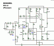
Introducing the PX , tandem single ended.
I finally made my pioneer M-90 simulation "sing" . Based on the pioneer M-90 , the PX uses one differential to drive another. This does 2 things , the input stage is totally isolated from the voltage stages miller effect and the gain is VERY high (over 110db @22 Re).
THD wise it just slightly beats out the AX (blameless) at THD20K with .006%/20v p-p. At 500hz to 10k ... WOW... .00008% or below is typical. FFT wise.. same story H3/5/7 is about 120db below primary. One FINE AMP. 🙂🙂
One might describe this as the absence of higher order distortion , at 120v p/p we are still down below 90DB with .007-8%THD which NONE of the others can do. Also , according to the phase plot this amp is 90 degrees out of phase all the way from 20HZ- to the unity gain point (UG).
The strange thing is how Pioneer compensated this topology. They use a 5600pF/100R RC shunt between the first differential's collectors and gross global lead compensation. NO typical miller compensation at the Voltage stage
It also does not need to hunt for an operating point .. direct newton all the way (an easy sim). Still trying to wrap my head around this , but I have a 1mhz UG point with 97 degree phase , this would/should? not oscillate
(even with 100+DB gain 😀 ). Below is schema and simulation. Another "rabbit hole" to go down , or maybe dig another one... 😀
OS
Attachments
- Home
- Amplifiers
- Solid State
- The MONGREL (supersym II)