I have opended a webpage to insert all the information about this project
DAC End - the AD1865N-K with single ended vacuum output stage
I don't know how far along you project is but if you could stack or run the 1865's in parralel you could minimize the value of the IV resistor and keep the 1865 well away from its max compliance voltage.
Love the single ended stage
Same as Jonners i'd be interested in an 1865 board with an I2S converter as my interest in spdif is close to zero.
Agree, the S/P-DIF does absolutely nothing good for music reproduction IME!
I made an experiment many years ago using a Teac VRDS P700-CD-drive and an external DAC (LC Audio ZAPdac).
Took out BCLK, WCLK and data directly from the drive and re-shaped the signal. Removed the oscillator from the P700 and used only the low-jitter clock in the DAC as master.
I was totally shocked about the improvement! Since then I've only used integrated CD-players (SONY SCD for SACD-playback) but now only interested in the sound of my non oversampling usb dac.
You get tons of bit errors out of old CDs...
So the true DACEND will have to include a USB-interface IMHO. ;-)
Nice project & a nice thread anyway.... ;-)
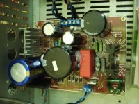
AD1865 is great dac, easy to make , high quality sound
i have sample dac project with ad1865
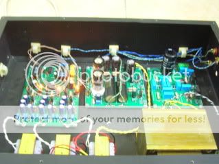
first protype, i use simple regulator for dac, and srpp for iv
then i'm replace srpp iv by paraller triode iv
second ver i use shunt regulator for dac board
b.r
i have sample dac project with ad1865
first protype, i use simple regulator for dac, and srpp for iv
then i'm replace srpp iv by paraller triode iv
second ver i use shunt regulator for dac board
b.r
Last edited:
AD1865 is great dac, easy to make , high quality sound
i have sample dac project with ad1865
first protype, i use simple regulator for dac, and srpp for iv
then i'm replace srpp iv by paraller triode iv
second ver i use shunt regulator for dac board
b.r
Great samples, guy. It seems that shunt regulator is the rule of success in efficient power supply for DAC. And parallel triode at I/V stage is a saver for extended bandwidth output.
Suggest you to try the shunt power supply board by Quanghao, the more completed and tested one, with your DAC part to see how things are changing.
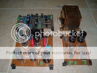
On the AC side, can we have a photo of your transformer? Thanks for sharing.
Last edited:
thanks mr vancao, i know quanghao shunt regu, but it is hard to find part. for that reason i don't make it
my new project is active reduce noise for dac supplier
PS: tranformer is my diy product
b.r
my new project is active reduce noise for dac supplier
PS: tranformer is my diy product
b.r
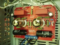
AD1865 is great dac, easy to make , high quality sound
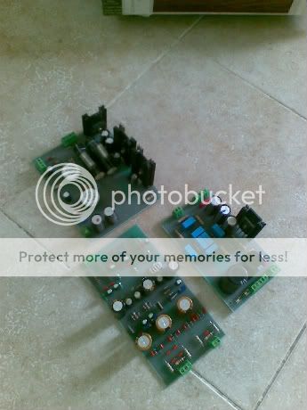
i have sample dac project with ad1865
otc 2009 ver
2008 ver
first protype, i use simple regulator for dac, and srpp for iv
then i'm replace srpp iv by paraller triode iv
jan 2009 ver
second ver i use shunt regulator for dac board
b.r

How many mA must the 12v line(each of the 12v lines) be able to deliver to the Salas shunt pcb?
How many mA must the 12v line(each of the 12v lines) be able to deliver to the Salas shunt pcb?
about 250-300ma for on the 12 V line!
Hi Quanghao,
Are the DAC and Salas boards still available ? Could you give me the ordering information ( prices and paypal address )
Mark
Are the DAC and Salas boards still available ? Could you give me the ordering information ( prices and paypal address )
Mark
Hi Quanghao,
Are the DAC and Salas boards still available ? Could you give me the ordering information ( prices and paypal address )
Mark
No! I think I will make it later! When i will sent all PCb of DAC.
Now I have only PCb of Salas for DAC and PCb IV stage 5687 for Dac or for Pre!
Thank you!
Quanghao
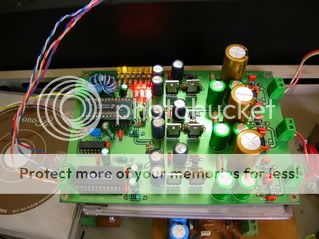
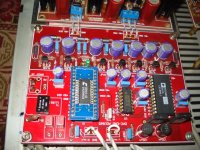
Now im layout new PCb for DAC-end use trasformer for output, all in one PCB, and i change tl431 by many Salas shunt low!
with capital under $ 1000, DAC-end can be compared with any DAC that cost $ 5000. is my thought! and when you've completed it you find difficult to replace the DAC that the present time and the next few years.
Im sure I will take a long time for the best layout
with capital under $ 1000, DAC-end can be compared with any DAC that cost $ 5000. is my thought! and when you've completed it you find difficult to replace the DAC that the present time and the next few years.
Im sure I will take a long time for the best layout
Now im layout new PCb for DAC-end use trasformer for output, all in one PCB, and i change tl431 by many Salas shunt low!
with capital under $ 1000, DAC-end can be compared with any DAC that cost $ 5000. is my thought! and when you've completed it you find difficult to replace the DAC that the present time and the next few years.
Im sure I will take a long time for the best layout
Do you have a schema of it?
Why do people keep using SRPP tube outputs on DAC's?
Because people like it. It's simple, easy to build and almost no need to worry to much about the bias when changing tubes. Most important, it gives you a reasonable good sound compared to other circuits in similar investment.
They are push-pull and get very unbalanced with the load (input impedance of the amp.)
What is the meaning of "Very unbalanced with the load"? Why does it is unbalance with the load? Do you mean load mismatched or something else?
I've comapred several tube outputs for DAC's and nothing sounds better with the right tube in a simple grounded cathode. Its SET and with the right tube can power any amp with a reasonable input impedance (40kohm or higher.)
The other issue with the AD1865 is the low output current you are going to use a high resistance I/V resistor which is not good. Best to parallel 4 AD865's to get a higher current and less load on the DAC Chip.
Why a high resistance I/V resistor is not good? V=IR is the Law of Physics. To get the desired level of signal, you can either increase the value of current source or the value of I/V resistor, provided that it's not too big to be affected by the input resistance of the next stage. The input resistance of the tube output stage is greater than hundreds Kohm whic is not a factor.
As far as the load dependance of SRPP read Broski'es article on SRPP. I did a lot of experiementing with SRPP in DAC's and found that a simple 6n6pi or 5842 with output taken from the anode sounds a lot better, just personal experience and Broskie does a good job explaining the why.
As far as bigger I/V resistor there is proof that most R2R DAC sound best with the lowest I/V resistor possible, some claim the AD1865 is somewhat immune but the datasheets are not specific. Basically you want the DAC chip to see the lowest impedance possible, this is why people spend hundreds of hours designing low ohm analog stages for DAC's like Jocko's I/V, etc.
can you sent the circuit???
thank
I used a PCM63 so I used this simple stage with a 47 ohm I/V resistor:
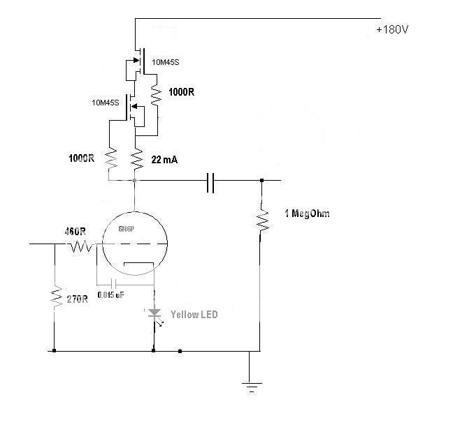
But I am now working with an AD1862 which has similiar +_1mA output as the AD1865,
so I am going for a lower I/V resistor (10 ohms) and a gain stage of 100, output impedance is 800 ohms:
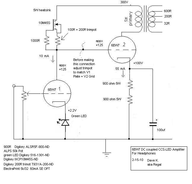
Except no output transformer (just CCS like the first stage & OTL 1 uf cap) and the led on the first stage is upside down (I need to correct that), may experiement with cap coupling stages and grid bias on the second stage per Sy's recommendation. I'll report how it works out. I will modify the schematic for DAC output if there is interest. But this gives you the general plan.
But I am now working with an AD1862 which has similiar +_1mA output as the AD1865,
so I am going for a lower I/V resistor (10 ohms) and a gain stage of 100, output impedance is 800 ohms:
Except no output transformer (just CCS like the first stage & OTL 1 uf cap) and the led on the first stage is upside down (I need to correct that), may experiement with cap coupling stages and grid bias on the second stage per Sy's recommendation. I'll report how it works out. I will modify the schematic for DAC output if there is interest. But this gives you the general plan.
Last edited:
- Status
- Not open for further replies.
- Home
- Source & Line
- Digital Source
- AD1865 the best DAC