Hi Dave,
I think you're going to roast the 6EW7... quiescent current is more than the max. plate dissipation for each section of this tube. I would 1/2 the plate current.
I think you're going to roast the 6EW7... quiescent current is more than the max. plate dissipation for each section of this tube. I would 1/2 the plate current.
Hi Dave,
I think you're going to roast the 6EW7... quiescent current is more than the max. plate dissipation for each section of this tube. I would 1/2 the plate current.
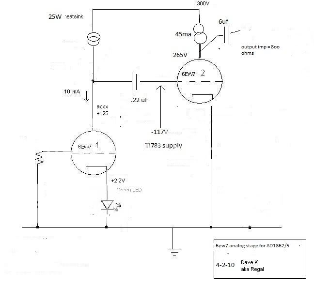
Yes, I have a better operating point which is just under max plate dis @45 mA, should read 265V plate 117V grid, 100V cathode (7.5W dissapation 10W max). If you look at the datasheet the Rp climbs real fast as you get away from max plat dissapation, wanted to keep it near the 800 ohms for min output impedance.
And yes the intention is no OPT for the line stage, and CCS loading the second stage instead so a less expensive PS would be needed.
This is the schematic I ment to post. close to 100x gain and 800 ohm output impedance, allows 10-15 ohm I/V resistor with AD1862/5. On my plate to build for my PMD100-AD1862 DAC.
Last edited:
looking good so far. are you going to use a dn2540 cascode or something similar?
What are you going to use for IV resistors? If you are going all out then i can recommend texas components (nothing to do with texas instruments). good service and very very tight matching.
What are you going to use for IV resistors? If you are going all out then i can recommend texas components (nothing to do with texas instruments). good service and very very tight matching.
looking good so far. are you going to use a dn2540 cascode or something similar?
What are you going to use for IV resistors? If you are going all out then i can recommend texas components (nothing to do with texas instruments). good service and very very tight matching.
yes dn2540 cascode. Digikey carries high quality resistor Caddock series TO-126 resistors that I will probably use.
Only concern is the small input signal and noise may be a problem, but I have tried stepup transformers like audionote uses in the past and didn't like their sound coloration. This is basically like making a phonostage for a DAC minus the eq circuit.
There are a couple typos on my schematic. grid bias should be -17V, plate voltage after the CCS 165V. Sorry.
recloking and dual AD1865 parallel
I had some questions about this design.
1. Way this DAC relay on clock from SPDIF and not using reclocking? How difficult is to add reclocking? Will reclocking improve jitter on this DAC?
2. What changes must done in schematic of digital side to use dual AD1865: L and R channels of one chip in parallel?
More questions:
How rigth/wrong is information on site: Retro - DAC adout digital schematic of this DAC:
"all non-oversampling DACs have the same bug... At the recording side samples a made at the same time. Now look at CS8414 chart. We've got serial output: first goes out left channel, than right channel with 32 clock-beatings delay (signal FSYNK), which is T=1/(2*Fsmp) = 1/(2*44100)= 11.34 microseconds. It produces the phase shift between the channels:
360* 1000*0.00001134=4.08 degrees @ 1 kHz
and :
360*20000*0.00001134=81.7 degrees @ 20kHz."
dac going to conversion just after accepting two words L and R...
not left after received left data word and so...
I think that is not true...😕
not left after received left data word and so...
I think that is not true...😕
I have up dat for DAC-ENd2.
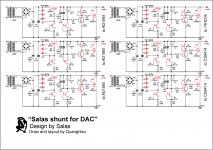
i change all Tl 431 by Salas low shunt. you can se the circuit
i change all Tl 431 by Salas low shunt. you can se the circuit
Attachments
Last edited:
that is going to be an expensive build, with a lot of tranformers! I like the idea though.
yes i se. but that is very good for this DAC
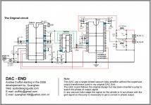
I've been working with this AN dig board for many years and just built one without half the junk AN put in. You have to be aware that it was not AN UK that designed it but their kit guy back then.
Glad to see you removed the digital filters in later versions of your board. I found the best sound was to come right off the 1865 using a good I/V transformer to a tube buffer out as shown in later examples. I agree SRPP sucks in this case.
I would be very interested in getting one of the dac board and shunt power supply.
BUT what I would be most interested in is developing a battery supply using A123 batteries for the board.
At one incarnation of the FrankenDAC (my name for my two box monstrosity) I could switch battery or AC power. On battery it was STUNNING. However using 3 SLA batteries had its problems which was no dynamics to speak of but wow how quiet and delicate!
The problem for years is SLA batteries are a bad choice just as car batteries are for filament supply. Now with these new A123 batteries they have a impedance of .008 Ohms..
Next if someone could really show a proper schematic to implement I2S into the 1865 that would be a huge leap and allow removal of the receiver chip.
Finally feeding with the M2Tech from computer audio modded to use battery 3.3V for their clocks and I2S output.
NOW you geniuses if you can come up with that it will destroy most dacs you've ever heard for a fraction of the price.
I've built many dacs over the years and keep coming back to the 1865 chip as the most musical and natural. The idea is to refine the circuit to make its as simple and efficient as possible.
I have up dat for DAC-ENd2.
i change all Tl 431 by Salas low shunt. you can se the circuit
Where are the output electrolytics? Will oscillate without.
I've been working with this AN dig board for many years and just built one without half the junk AN put in.
Hello phrarod
Maybe you know:
1. Why this DAC relay on clock from SPDIF and not using reclocking? How difficult is to add reclocking? Will reclocking improve jitter of this DAC?
2. What changes must done in schematic of digital side to use dual AD1865: L and R channels of one chip in parallel?
dac going to conversion just after accepting two words L and R...
not left after received left data word and so...
I think that is not true...😕
Not exactly this way. After reading CS8414 and AD1865 data sheets carefully I find out that there is delay between channels. On AD1865 "The falling edge of LL and LR cause the last 18 bits which were clocked into the Serial Registers to be shifted into the DACs, thereby updating the DAC outputs." The LL and LR are taken from CS8414 FSYNC output. To get falling edge on LR, when on DL (also DR, serial data inputs from SDATA on CS8414) right channel data data is clocked into the input registers, FSYNC is inverted. Result is 32 clock-beatings delay for right channel what causes 4.08 degrees @ 1 kHz and 81.7 degrees @ 20kHz phase shift.
This happens also on the DCA End 2.
I had not yet analyzed AudioNote schematic between 8414 and 1865 but I think it is better.
Sorry, can't catch your thoughts.... what phase shift and 32 sck delays ?
CS8414 serial out works in mode 6 (L/R, 18Bits LSBJ). Because data is LSB left justified, we have 14 sck cycles before MSB shows up (32 sck in whole audio sample). FSYNC goes directly to left channel latch. So no problems there whatsoever (timing between LSB ant FSYNC falling edge is in accordance with datasheet) . Now right channel latch gets inverted FSYNC with cmos propagation delay (in my case using ST HC04, ~16ns). This has no impact to transition beginning, because of 14 sck cycles before MSB. Now whole sample is fed to DAC, FSYNC goes up, inverts, gets delay from inverter, latches the Right channel DAC with normal delay of "LSB to FSYNC" + 16ns, end of story.
Am I missing something ?
Dunno about Audionote, but there were HC04 in between 8414 and 1685 in some version fur sure. Post a link to some reliable schematics if you know one.
I went through the documentation of the chips, very informative !
Why the CS8414 shown bi-phase coding error in my DAC_END ? Is it supposed to be like this ?
I am very tempted in doing a cute front panel showing the status leds, but I understand I would need a reference frequency to have info in the signal frequency.
D.
Why the CS8414 shown bi-phase coding error in my DAC_END ? Is it supposed to be like this ?
I am very tempted in doing a cute front panel showing the status leds, but I understand I would need a reference frequency to have info in the signal frequency.
D.
I went through the documentation of the chips, very informative !
Why the CS8414 shown bi-phase coding error in my DAC_END ? Is it supposed to be like this ?
I am very tempted in doing a cute front panel showing the status leds, but I understand I would need a reference frequency to have info in the signal frequency.
D.
My be some CS8414 have wrong,
You can conect Jump pin 1 to 2 . Note : led turn on and turn off!
- Status
- Not open for further replies.
- Home
- Source & Line
- Digital Source
- AD1865 the best DAC