I haven't tried to run it from the center yet. I think it will work. But, how would I inject the signal between the emitters in keantoken's scheme?
Merely join the drive currents together, and with Allison's reference center.
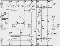
This is one way. With bootstraps I can now output within 2V of either rail.
I'm unsure why it konks out at only +/-22V??? I was expecting a Volt more.
This sort of thing only happens when you try to show someone...
Now Zeniers become necessary to protect the gates. Maybe I shoulda done
that in the first drawing too? But definitely with strapped gates you gotta.
Put in a signal that clips, no Zenier, straps could pull the gate to 36V easy!
Obviously the source can't swing with it above the rails.
Attachments
Last edited:
And what happens to output transistors when/if it clips? Maybe its just a gate thing...
But there's a reason why I strap from what doesn't at first seem the sneakiest place.
Storing a charge into the drive signal messes with both clipping and crossing behaviors.
Can still do it your way, but may have to increase quiescent currents to insure neither
transistor gets turned off.
Remember, you gotta pump equal current swing into those boot caps coming and going.
The flipside of that wildcard, bootstrap totems are most optimum when equal resistors
are used. So, why R1/R5 different?
Why is it an advantage the bootstraps be "more CCS like"? There is nothing linear about
two high impedance currents crashing into each other without a load to soften the blow.
There is no special linearity in the amount of current required by the Darlington's base.
Is true CCS an actual advantage? Or we have just assumed somehow it must be?
Last edited:
Your transistor can turn off whenever the bootcap unfortunately happens
to cooperate in pulling the output a direction the Allison also wants to go.
Which sounds like a good thing, except your transistor just turned off!!!
Unless the bias currents are made significantly higher than boot currents.
Tail wags the dog too, it so happens. Clip it and/or AB it and see how it
exaggerates the mess.
Maybe a true CCS in place of the collector resistor in the totem would
prevent some of that reverse waggage.
Last edited:
I don't understand what you say about bootstrap resistors being equal. One always has a constant voltage across it and the other is taking all the AC from the cap. Why not make the higher resistor a higher value so that the cap passes less AC? Or vice-versa, for better bootstrap output impedance?
I've looked at clipping behavior and it's nothing alarming. The thing is, a mediocre bootstrap will decrease input impedance dramatically, lower OLG and increasing distortion, not to mention the distortion added by the odd bootstrap currents (wobbly triangle).
Downside is, R6 has to be decreased to keep up with the bootstrap currents.
- keantoken
Make the top resistor too small, the caps work harder and the boot doesn't
swing true to the output. Make the top resistor too big, it can't charge the
cap as fast as its being depleted. You can't have it both ways and the best
compromise almost always turns out to be equal resistors, unless you got a
special reason why one needs to be different (non 50/50 duty cycle etc...)
I can't think of any logical exceptions that apply here.
Last edited:
Make the top resistor too small, the caps work harder and the boot doesn't
swing true to the output.
We can just make the cap larger.
Make the top resistor too big, it can't charge the
cap as fast as its being depleted.
No DC current flows through the cap; the values of both resistors are chosen so that the appropriate amount of current flows. If the top resistor is too big then you'll simply have less current than you were aiming for. And it's not the top resistor that drives the cap, the cap drives the resistor.
You can't have it both ways and the best
compromise almost always turns out to be equal resistors, unless you got a
special reason why one needs to be different (non 50/50 duty cycle etc...)
I can't think of any logical exceptions that apply here.
It is a compromise between cost and quality. A different ratio might work better but it's up to you whether some extra uF is over your budget.
- keantoken
The two resistors in series have some arbitrary required value.
Pick any node within that resistor to tap in the bootcap.
The optimum spot is always the middle. Always. Almost always.
Most of the time, usually, unless its Tuedsday at the equator
and the Earth's field flips pole to pole....
Not cost vs quality dude. Its in the same vein as impedance
match, or maximum power transfer. Its just basic electronics.
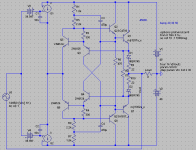
Don't know what I'm doing wrong here... I've attempted to sim the latest and get this. I tried it with the zener and moving the bootstrap cap connection to Ken P's location with the same result.
OK, so maybe you can get away with it. So long as you are abusing a CCS.
I still think quiescent voltage drops should be about equal, for the biggest
voltage boost with the smallest bootcap. But no probs for the CCS to have
much higher dynamic resistance than the railside resistor.
But in this case, I'll never need to swing this drive to 36V. I need only about
5V beyond the rails. So I'm now dropping more than half my quiescent Volts
into a 1K8 railside resistor. Breaking my own rule, but imbalanced completely
the opposite way of where Keen is going with the smaller railside resistor.
As for oscillations like the klewis post above: I find it helpful to round all the
corners of the simulation, and shield my entire keyboard with tin foil...
And here's a zip with .asc files of my last three sims.
CHK = Outside driven, CHK1=Inside w boot, CHK2=Inside w boot and CCS.
Won't need any extra libraries but an up to date LTSpice.
Attachments
Last edited:
As for oscillations like the klewis post above: I find it helpful to round all the
corners of the simulation, and shield my entire keyboard with tin foil...
Tried that already, other thoughts?
😕
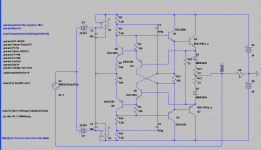
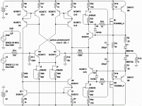
Kenpeter, take my schematic in post 462... Make R5 1k and R1 3.3k.
Now the cap works less while pumping through R1's impedance. The only downside to this is the decreased output impedance. How is this not optimal?
Klewis, I got the same simulation results... I don't know why it's doing this. If all else fails, try moving the bootstrap references to the bases of Q4 and Q6 (although this is simulation, it is not necessarily like it is). (by the way, there is no compensation in that schematic - why not add it and then see?)
- keantoken
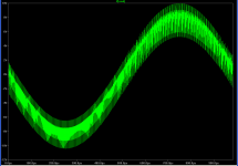
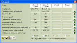
Allison v6 up and running. 😛 51pf compensation, no oscillation. Square wave decent at 20kHz; some slope, a bit of rounding, no overshoot. Zobel not attached for these test. Bias resistor for the drivers set at 475ohms, they don't get hot, will test with the resistor reduced to 300 next. Resistor between Allison pair emitters at 200ohms. Heat sink gets warm but not hot, will try reducing it to 150. Drivers are MJD243/253s, output transistors are 2sc5200/2sa1943. Measurements with sound card set at -26db input.
Ken P, are you using the oven weight foil or the regular thickness?

Ken P, are you using the oven weight foil or the regular thickness?
Attachments
The secret is real tin, none of that aluminum feldgercarp...
Darn, I was afraid you would say that, don't have any of that on hand...
Without having to resort to "tin" I was able to get the following to simulate without oscillation. When I make R5/R6 larger, say 90 ohm each, it reverts to oscillation. Also, if I set C1/C2 to 50p it oscillates.
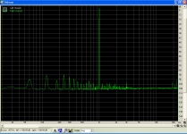
I went ahead and modified V6 to match this schematic with the exceptions of the resistors and caps mentioned above and mjd243/253's for the drivers (couldn't get them to work in the sim - oscillated). V6 is the last posted results, which seemed pretty good. I got to thinking that the low hz harmonic spikes are all multiples of 60 hz. Because the amp is running in class A is this power supply ripple coming through? I have a pair of 47,000uf caps in the supply, but only one cap per rail.
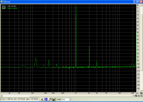
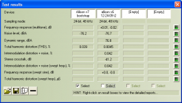
I'm calling the bootstrap Allison V7. The result for V7 were not as good as V6, .036 THD vs .0046 THD. But, V7 had fewer low hz harmonic spikes but, a large harmonic at 2kHz. Maybe the low hz harmonic spikes were damped out by the 1,000uf caps of the bootstrap?
So, I'm thinking there's not much benefit to driving the Allison between the Allison emitters, seems the outside drive is just as good if not better. I'll post the THD plot later today.
Last point on this post, Ken Peter, I drove the Allison V6 to the rails without clipping - I used the LME49811 to drive both the Allison and my double CFP into clipping. Both took the same amount of 1k sine wave before the bottom portion of the wave started to flatten. Maybe you're seeing a simulation artifact?
Ken L
I went ahead and modified V6 to match this schematic with the exceptions of the resistors and caps mentioned above and mjd243/253's for the drivers (couldn't get them to work in the sim - oscillated). V6 is the last posted results, which seemed pretty good. I got to thinking that the low hz harmonic spikes are all multiples of 60 hz. Because the amp is running in class A is this power supply ripple coming through? I have a pair of 47,000uf caps in the supply, but only one cap per rail.
I'm calling the bootstrap Allison V7. The result for V7 were not as good as V6, .036 THD vs .0046 THD. But, V7 had fewer low hz harmonic spikes but, a large harmonic at 2kHz. Maybe the low hz harmonic spikes were damped out by the 1,000uf caps of the bootstrap?
So, I'm thinking there's not much benefit to driving the Allison between the Allison emitters, seems the outside drive is just as good if not better. I'll post the THD plot later today.
Last point on this post, Ken Peter, I drove the Allison V6 to the rails without clipping - I used the LME49811 to drive both the Allison and my double CFP into clipping. Both took the same amount of 1k sine wave before the bottom portion of the wave started to flatten. Maybe you're seeing a simulation artifact?
Ken L
Attachments

It looks to me like wraparound drive is better too. Emitter drive is has issues, especially with bootstrapping, which I think about halves the current gain or even more depending on where you bootstrap, which depends if you can get it stable (I'm still not sure why it's not stable). I seriously doubt the benefits, if there are any, would be an excuse to add 4 more transistors to the circuit.
Thing is, Klewis, without decently large R5/R6 the diodes will have no bias and it is operating in pure class B - far, far from optimal. May I suggest you put a 22uF cap between the emitters of Q8 and Q9? This will minimize the affect the emitter resistors have on the AC OLG. For that matter may I also suggest that you replace R5 and R6 with the same type of schottkeys, and then the diodes will have a realistic minimum bias voltage. Then to increase the bias you can put resistors in series with the new schottkeys if you want to.
Regarding V6, in the simulator it has a THD sweet spot where THD is roughly even regardless of power level, at around 100mA bias. (you might also try the capacitor tweak from the above paragraph, but I haven't mentioned it thus far because I did't expect it to have an affect - I'm realizing now that it may affect stability for better or for worse)
Also, at this point how do the Allison variations compare against the normal EF Darlington output stage?
Again I thank you for your tests,
- keantoken
It looks to me like wraparound drive is better too. Emitter drive is has issues, especially with bootstrapping, which I think about halves the current gain or even more depending on where you bootstrap, which depends if you can get it stable (I'm still not sure why it's not stable). I seriously doubt the benefits, if there are any, would be an excuse to add 4 more transistors to the circuit.
Thing is, Klewis, without decently large R5/R6 the diodes will have no bias and it is operating in pure class B - far, far from optimal. May I suggest you put a 22uF cap between the emitters of Q8 and Q9? This will minimize the affect the emitter resistors have on the AC OLG. For that matter may I also suggest that you replace R5 and R6 with the same type of schottkeys, and then the diodes will have a realistic minimum bias voltage. Then to increase the bias you can put resistors in series with the new schottkeys if you want to.
Regarding V6, in the simulator it has a THD sweet spot where THD is roughly even regardless of power level, at around 100mA bias. (you might also try the capacitor tweak from the above paragraph, but I haven't mentioned it thus far because I did't expect it to have an affect - I'm realizing now that it may affect stability for better or for worse)
Also, at this point how do the Allison variations compare against the normal EF Darlington output stage?
Again I thank you for your tests,
- keantoken
keantoken,
I think V6 may have the most promise. I'm still learning about my test setup. As everything is open with the wires not carefully routed, my results aren't as consistent as they should be. I went back to see if the original Allison - full class A Paul's scheme - which has 1000uf caps on the board bypassed with .1uf polypropolyne would measure better in the lower hz areas. Moved a few wires, taking care to hold them away from others and got rid of the 2khz harmonic. The lower hz harmonics are also minimized. This Allison is being driven from the top and bottom as well. Seems like the simplier scheme to be explored further. I cut V6 up pretty badly to make it into V7, so, will remake it with onboard 1,000 uf caps. I've posted the results below. The first one is V7 and the second is the original Allison. And interestlingly enought it uses MJE15032/33's as the drivers. It's basically running at the THD threshold of the LME49811.
So, right now, in the Allison A/B typology, the V5 - no resistor between the Allison emitters and two pair of diodes and .1 Re's between the output resisitors has measured as well as the CFP stage. My next challenge is to tune up the LME - I had one version running at .0036 Thd but it's got messed up with all the testing. I plan on going back and reworking it to try and get the good results again.
Attachments

- Home
- Amplifiers
- Solid State
- Simulation Analysis of several unique Allison-based output stages.