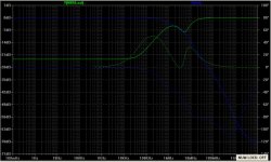
Those results are actually very optimistic... Response get strange a bit after 10GHz, think it'll oscillate at those frequencies? 🙂
The feedback circuitry is SPICE modeled, and so it'll be very optimistic in comparison with real life... Don't expect it to work that well at even 1MHz.
But so far, looks healthy to me. (if you want to see in detail the stability of the Allison, probe between the emitter of Q8 and the output)
- keantoken
At frequencies over, say, 100 MHz you need to include parasitic inductance and capacitance of wires, traces, etc. In addition, the BJT model is not adequate as higher order effects begin to become significant.
In reference to Ken L's latest... I'd probably throw 4.7K~10K Ohms in parallel with C1
and C2. I find it stabilizing that Allison error correction be allowed some slack even
at DC... It "distorts" a little more when the error correction isn't forced rigid, but the
distortions favor much lower orders. An error voltage gain of x10 or x20 is far more
than enough at the collector, it doesn't need or benefit to be theoretically infinite...
And I'm assuming you are gonna wrap the output back into an op-amp anyway.
Less unfixable glitchy wierdness back into GNF loop is the benefit of what I propose.
Last edited:
But so far, looks healthy to me. (if you want to see in detail the stability of the Allison, probe between the emitter of Q8 and the output)
- keantoken
keantoken,
Are you suggesting probing the simulation? If so, can you give more detail, with a tran analysis or ac, what would the probe equation be? Trying, to learn...
Thanks,
Ken
Yes, in simulation, AC analysis.
Click and drag from Q8's emitter to the output node. This measures the difference between those two signals, just like a differential scope plugin. The correct probe equation will automatically be entered.
- keantoken
Click and drag from Q8's emitter to the output node. This measures the difference between those two signals, just like a differential scope plugin. The correct probe equation will automatically be entered.
- keantoken
Yes, in simulation, AC analysis.
Click and drag from Q8's emitter to the output node. This measures the difference between those two signals, just like a differential scope plugin. The correct probe equation will automatically be entered.
- keantoken
Here it is.
Attachments

Wow, that is odd looking...
Well it doesn't oscillate in the .tran analysis so it can't be bad, perhaps the weirdness is just a result of it being used oddly (the response peaking is worrisome though - why would it resonate at 50Hz, then 10KHz, then 1.5MHz?). I'm not sure but I wouldn't expect it to behave this way in the real world.
Well, you have a working circuit, what modifications do you want to do next, or is this the end of it?
- keantoken
Wow, that is odd looking...
Well it doesn't oscillate in the .tran analysis so it can't be bad, perhaps the weirdness is just a result of it being used oddly (the response peaking is worrisome though - why would it resonate at 50Hz, then 10KHz, then 1.5MHz?). I'm not sure but I wouldn't expect it to behave this way in the real world.
Well, you have a working circuit, what modifications do you want to do next, or is this the end of it?
- keantoken
Played music on the class A version all day today. Used a window fan to keep it cool. 🙂 Sound was great!
Well, I going to build it this week and see what happens. Busy laying out the board. Hope to etch it tomorrow after work. I'll let you know.
Ken
On that note, I just realized why it was so weird - it is in fact acting completely as expected. Your reactive speaker model is what's causing the response strangeness.
Nothing to worry about at all, it is expected.
Good luck and I'm glad it sounds good. 🙂
- keantoken
Nothing to worry about at all, it is expected.
Good luck and I'm glad it sounds good. 🙂
- keantoken
On that note, I just realized why it was so weird - it is in fact acting completely as expected. Your reactive speaker model is what's causing the response strangeness.
Nothing to worry about at all, it is expected.
Good luck and I'm glad it sounds good. 🙂
- keantoken
Simulation into a simple 8 ohm load.
Attachments
Klewis,
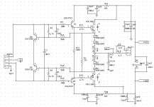
If you want to modify the Allison output stage to be a Class AB amplifier, then the attached circuit shows how. Adding two schottky diodes and reducing Re to 0.1 ohms will give a bias current of 360mA (it will start at 260mA with cold diodes). The OnSemi model for the mbr1045 and LTspice will indicate a bias current of 460mA, but it is actually 360mA.
Note the following:
- Two schottky diodes (mbr1045 or mbr745 would be good choices) and added to each Re emitter resistor. This (and Re3) is a modification to one of Kenpeters designs of some time ago.
- Re3 (33ohm) is used as a `keep alive' current to keep the output transistors, drivers and Allison bias transistors always on (and this is a good thing).
- Rf is moved to provide overall feedback, as the Schottky diodes increase the distortion such that some feedback will be required to reduce it.
- Ccomp stays on point X.
The two schottky diodes give a very smooth transition from conducting to non conducting, and hence produce less high order harmonics than normal (another good thing). If you want to model this, the OnSemi mbr1045 spice model is the closest that I could find to actual devices.
The Allison bias transistors should be thermally bonded to schottky diodes D1 and D4. Ksc3503 and Ksa1381 To126 transistors are good choices for these. Keep these diodes and Allison bias transistors away from the output device heatsinks, and ventilate well. Try to keep them at a constant temperature.
The bias current of 360mA will give Class A operation up to about 4 Watts into 4 ohms with quite low distortion. Most music is below 4 watts.
I suggest you try to get the Class A version working first, then add the Schottky diodes and Re3.
I hope this is of interest.
Paul Bysouth, Nov 2009
So, it's built and running. The attached is the schematic. Measured 1.140v Emitter to Emitter at output transistors - it was cold out (well for Southern California). This voltage was rising at about 1mv per 5 seconds. The simulation shows 1.17v for this. Sine wave looked smooth, but, the 1khz square wave had a fair amount of overshoot and the 10khz square wave had an overshoot almost equal the height of the wave. The measurements were taken with an 8 ohm load attached. I also tried reducing the signal generator input voltage to 5 mv to try to simulate sub 4 watt class operation (no math attempted just a guess on input voltage) but, no change.
I'll take photos of the scope tomorrow night.
On the positive side the heat sink wasn't even starting to heat up.
Any thoughts on how to kill the overshoot?
Ken L
Attachments
The traditional way of killing overshoot would be to increase compensation somewhere...
The overshoot is either coming from the LME or from the Allison, I'm thinking the LME. Try increasing the 33pF caps on the Allison and if that doesn't help, increase compensation for the LME.
- keantoken
The overshoot is either coming from the LME or from the Allison, I'm thinking the LME. Try increasing the 33pF caps on the Allison and if that doesn't help, increase compensation for the LME.
- keantoken
So, it's built and running.
Any thoughts on how to kill the overshoot?
Ken L
Could you post the whole circuit?
Cheers
Could you post the whole circuit?
Cheers
Stinius,
The front of the circuit is back about 30 posts or so.
Ken
Last edited:
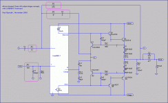
Klewis,
I have some suggestions for you to try:
1. The lme49811 data sheet has buried in it a specification for a minimum closed loop gain of 26dB (ie 20), and you have a gain of 19.1 To start I suggest you change the gain resistors to 1k and 27k giving you a gain of 28, which is very close to the THX standard of 28.2 (ie 29dB). Gains less than 20 "may cause instability"!
2. Referring to my attached diagram, I'd add resistor R2 and C2 which will have the effect of reducing the demanded gain at high frequencies and hence limiting the high frequency effect of the phase shift in the Allison output buffer. I'd start with `10pF < C2 < 100pF' and `0 < R2 < 1k'.
3. I also suspect that Ca1 and Ca2 (on my diagram) should be more like 100pF. 33pF seems a little low.
4. I'd start by connecting R3 (on my diagram) to point X (on my diagram) which will place the output buffer outside the feedback loop. Convince yourself that the lme49811 is properly compensated and that square waves don't have too much overshoot (monitor point X). Check that the Allison buffer is also handling square waves properly by monitoring point Y. Mixing square waves and a higher frequency sine wave, and mixing a triangle wave with a higher frequency sine wave are also good test methods (particularly for overload testing). Once all is well, then move R3 back to point Y.
5. I'd also add an input buffer (ie Ri1 and Ci1) to prevent high frequencies getting into the amplifier. Don't forget to allow for the preamplifier output impedance which will add to Ri1.
Could you also measure the bias current (with no load) through the Re1 and Re2 resistors please, both when cold and after operating for a while. Also how hot do the Schottky diodes get when in operation for a while?
Note on the attached diagram I've removed all the components that don't effect this discussion, but you'll still need them.
Please keep us updated with progress.
Paul Bysouth, Nov 2009
Attachments
Klewis,
I have some suggestions for you to try:
1. The lme49811 data sheet has buried in it a specification for a minimum closed loop gain of 26dB (ie 20), and you have a gain of 19.1 To start I suggest you change the gain resistors to 1k and 27k giving you a gain of 28, which is very close to the THX standard of 28.2 (ie 29dB). Gains less than 20 "may cause instability"!
2. Referring to my attached diagram, I'd add resistor R2 and C2 which will have the effect of reducing the demanded gain at high frequencies and hence limiting the high frequency effect of the phase shift in the Allison output buffer. I'd start with `10pF < C2 < 100pF' and `0 < R2 < 1k'.
3. I also suspect that Ca1 and Ca2 (on my diagram) should be more like 100pF. 33pF seems a little low.
4. I'd start by connecting R3 (on my diagram) to point X (on my diagram) which will place the output buffer outside the feedback loop. Convince yourself that the lme49811 is properly compensated and that square waves don't have too much overshoot (monitor point X). Check that the Allison buffer is also handling square waves properly by monitoring point Y. Mixing square waves and a higher frequency sine wave, and mixing a triangle wave with a higher frequency sine wave are also good test methods (particularly for overload testing). Once all is well, then move R3 back to point Y.
5. I'd also add an input buffer (ie Ri1 and Ci1) to prevent high frequencies getting into the amplifier. Don't forget to allow for the preamplifier output impedance which will add to Ri1.
Could you also measure the bias current (with no load) through the Re1 and Re2 resistors please, both when cold and after operating for a while. Also how hot do the Schottky diodes get when in operation for a while?
Note on the attached diagram I've removed all the components that don't effect this discussion, but you'll still need them.
Please keep us updated with progress.
Paul Bysouth, Nov 2009
Paul,
Thanks for suggestion. I will give them a try. Question on the output impedance of the pre-amp; I presume that it's value is set by the resistor at the output of the pre-amp, which as I recall is 100 ohms. I would therefore use 200 ohms (100+100) in the calculation to come up with Ci1. Or, is there a way to measure output impedance?
Ken
Klewis,
Yes the preamp output impedance just adds to Ri1 (ie 100+100). However I nomally just use LTspice with a simplified circuit to check that all the responses will be what I want. See the attached diagram. Note the effect the 15pF capacitor has on the loop gain at around 200KHz.
In your case, Ri1=1K and Ci1=220pF would produce a suitable filter assumming that the source impedance is 100ohm.
Paul Bysouth.
Attachments
success!
Here's the story - In parallel with making this output stage, I've been trying to get a EF stage to work with the LME49811 using the Thermal Trak output transistors with a bais scheme by Bob Cordell. Well I fired it up and after some serious head scratching - how hard could this be😱 - I found it was oscillating at 10Mhz. Funny, wasn't that the same frequency as the Allison. I put in a 0.01uf cap at the resistor between the emitters of the driver transistors, the same type driver transistors as the Allison. Fixed the occilation, but it still didn't work. So, I decided to swap out the driver transistors 2SA1837/2SC4793 (which were purchase from what I thought was a reputable dealer) for MJE15033/15032s. Fixed the problem, the EF stage runs great, flat square waves.
This got me thinking, could it be the 2SA1837/2SC4793s? So, I swapped them out for the MJE15033/15032s in the Class A Allison and removed the 100pf compensation caps. No oscillation, flat square waves, etc. Compensation doesn't appear necessary, note: the LME49811 feedback resistor is tied to Paul's point x, it doesn't wrap around the Allison.
I then swapped the drivers out in the Class A/B Allison - Paul's scheme. I haven't removed the 33pf compensation caps yet. It also worked, no more overshoot. As you might recall, the Allison is within the LME49811 feedback loop.
I haven't implemented any of Paul's other recommendation yet, but will in the next week or so, just for comparison sake.
Bad driver transistors?
Battery on camera was dead, so, pictures of the square waves will follow later today.
Paul, thanks for the latest spice example, made up one for myself, got the same results, which is always a good sign 🙂.
Regards,
Ken L
The claim to fame of the 1837/4793 are their speed for drivers - 100MHz. But the outputs are much slower than this - what, 20 to 30 MHz? 4MHz even? So maybe they were just "too fast".
I don't think they are bad, but rather, sometimes superfast japanese transistors and slower ONSemi types don't work well together.
Could you experiment a little more with the Allison compensation? There is a 10nF cap, then the 560 ohm resistors are still there (are they?)... Can you see which compensation caps are most important? I suspect that removing the 10nF cap will have a large affect. I'm interested here because the 100pF caps and 560 ohm resistors have the largest affect on THD20. If the distortion at this level is audible (many say it isn't), then reducing it should make the sound less "bright".
Thanks for your work,
- keantoken
- Home
- Amplifiers
- Solid State
- Simulation Analysis of several unique Allison-based output stages.