Dear Tube Gurus in this thread,
I have little experience with tube amps, but have a good understanding of general principles, and am all ears! I also have a fine ear and appreciate quality. I used to have a wonderful Heathkit tube amp that had a lovely warm sound on my full range quarter waves I made, but those got lost in a move ;-(
Please help me with a new project.
How it all started...
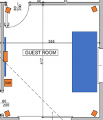
I have been experimenting with DML louspeakers of late and just love them. I started with Pink Pather Foamies, but rapidly graduated to warm guitar tonewood panels that round off that annoying edgy harshness of extruded EPS.
Now I read that DMLs are great for avoiding feedback, making them great for sound reinforcement. Techtonic Audio Labs who acquired the patents from NXT... So, curious, I tested mine with my Takamine N-10 with my sensitive Fishman neodymium pickup and my DMLs. Nothing, no feedback, not even with the amp cranked way up.
Sooo koool.
So, here is my project:
A stereo acoustic guitar tube amp in a DML briefcase format.
Not knowing much about tube amps, I bought some inexpensive ones to test, a stereo preamp (6J1) that I want to stack L+R for gain and overdrive (mono), and a 3+3W power amp (6P1, stereo).
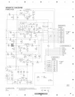
My proposed circuit diagram is here:
Dropbox - AcousticGuitarAmp.png
The preamp is a 6J1 type. No questions here, simple 12 VAC supply. Now, perhaps this preamp was not a good choice (perhaps even EQ'd for a phono pickup, oops!), most guitar amps use 12AX7s tubes, whatever... any ideas or suggestions on this appreciated?). The preamp is here (got it on sale):
aassembled ac 12v 1a 6j1 preamp tube preamp amplifier board preamplifier module pre-amp headphone bile buffer stereo bass hifi x10-d Sale - Banggood.com
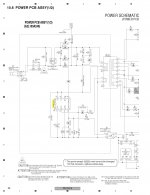
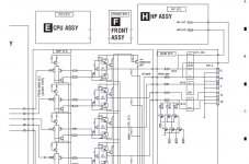
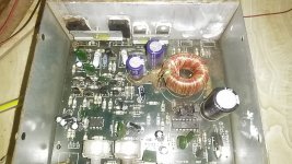
The question I have regard mostly the proper hookup of the the power amp, the classic 6P1 JCDQ-11
Many input voltages (0-230-230 and 6.3V), what appears to be options (diodes, a coil,..??) . Transformers (input and output) are mostly my issue.
Dropbox - JCDQ-11-6P1TubeAmp.png - Simplify your life
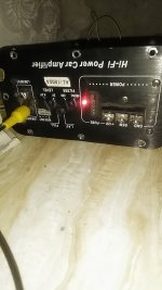
The power amp is to be found here (got it on sale):
jcdq11 tube amplifier 6n1+6p1 valve stereo amplifier board filament ac power supply + 3pcs tubes Sale - Banggood.com
Please advise. All comments, feedback, suggestions and warnings will be taken most seriously and they will be greatly appreciated. Many thanks in advance. Will share the results on INSTRUCTABLES if good.
Any hints where to get cheap reliable components will also be greatly appreciated. Such transformers appear to be quite specialized.
Many thanks in advance,
Paul.
Quebec City, Canada.


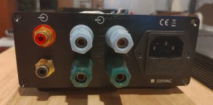

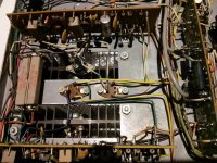
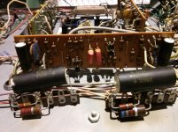

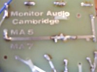

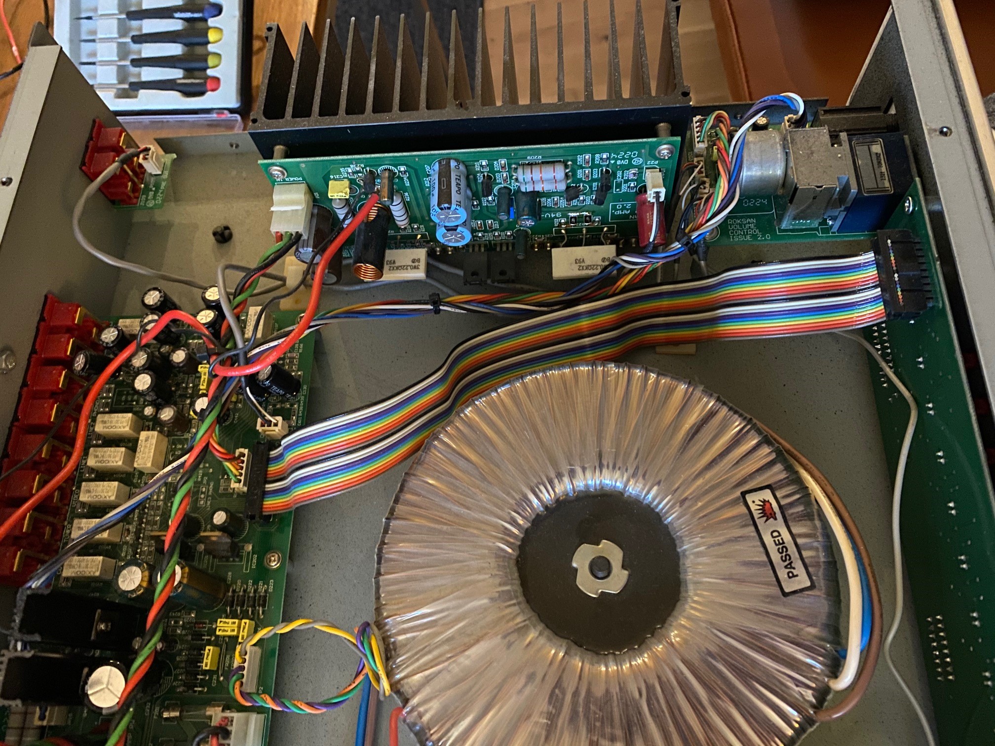
 , I would like to purchase and use a stereo power amp to run the subwoofers. Has anyone had experience with bypassing the T500 module to connect an external power amp? I haven't seen enough images that shows how the wiring is routed in the box to map out a modification like this. Since I am doing this for a family member, I don't have access to the cabinets to research my ideas. Any help would be appreciated.


