Hi
Everybody, I'm working on a Input and also Driver stage on a new Design for a Class A Amplifier.
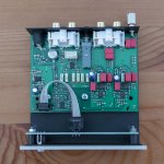
The Point is this input is already build and it is running almost perfect.
Now nothing seems to be perfect,sometimes. as you will see..
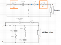
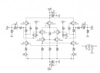
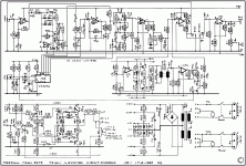
I'm trying to increase the upper Frequency range of that Stage. This consists of 3 Transistors. It can be two as well, but if I use only two then I lose gain.
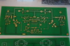
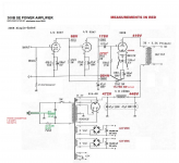
If I use three then Bandwidth will not Exceed 100Khz much. And output of Square Wave and also Sine wave will be Distorted, up to 1% comparing to 1Khz. The Circuit I have uploaded before already but I will upload it again, when I have Commented what has happen last night, in the circuit.
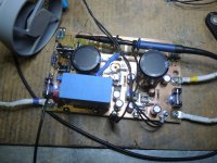
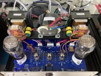
Now, this amplifier again with Output connected is build and it runs, but for my understanding there could be more. and has been tested already, and it sounds great, but I'm not finished with it yet.
Last night while testing and preparing the PCB, By accident, I reversed somehow the BASE and EMITTER Pins, of the first Drive Transistor. Put on my desk, plugged in my Test Equipment and tested just the output of the second Drive Transistor. This I tested OPEN LOOP, so none Negative Feedback as well Output Transistors weren't connected yet, and applied Power.
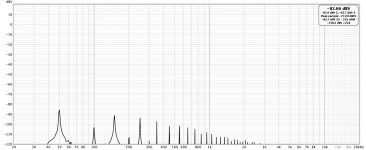
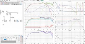
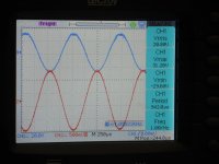
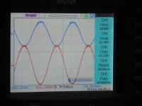
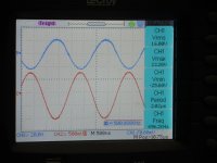
At that Time, this was last night, I didn't knew that I Reversed that Transistor, and started with 1KHz Sine Wave, and pulled up the Gain control on the Function Generator and measured Output on the Collector of the Second Drive Transistor with 25.6 Volt RMS! See Pic 10..
WOW!!! Why, what happen.??? I was stunned about that, so I viewed and controlled the RAIL VOLTAGES and there I thought I saw why, 48Volts, + and 48Volts -.
Oh, yes, of course, output Transistor hadn't been connected yet, OK clear.
So I connected a Load which would Simulate the Output Transistor to 70% and checked the Voltage again. DC V+- read both 43Volts sometimes only 42.9 but equal.
OK. Measured again the Sine and Square Wave of 1khz, still 20.8Volts output before the sine wave would really clip.
Switching the Frequency to 100KHz, again WOW, Clear as the 1KHZ Wave.
Turned Frequency up to 530KHZ till the output would drop down to 16Volts RMS. But no Clipping.
Slowly turned the function Gen backwards, and finally @300K there distortion was gone, and the full 20.0 Volts same as 1Khz where a there.
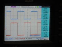
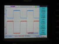
Now, it was still unbelievable. So I took a 1Kohm resistor and soldered this from Collector to GND.
Now some changes happened. But still 20Volts RMS output at the collector of the Second Drive Transistor. So, lowered that 1K to 600 Ohms and I still got 17Volts output.
So I was very pleased and measured Noise, and Hum and DCV out and all was better that I thought it would be.
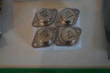
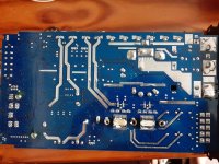
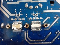
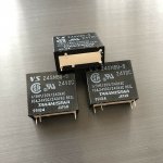
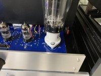
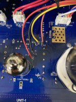
So, I decided to stop working on it, as it was already late night, and today I went back and checked everything because I thought I would connect the Power Transistors and the screwing the board on to the Heat sink. While getting the Drive Transistor in position to screw them onto the HEAT SINK, I saw something strange. The first Drive transistor had no number printed on front of it, or better say LABEL. I use BD139-10. this one are all PLASTIC.
So I took a multiplying lens and checked for the LABEL. and because of these two Transistors, are just besides each other I noticed that the thickness of the left one didn't match the right one, and then I looked at the backside of the left transistor, and there was the label. But hey, the amp was just running fine.
Connected the Amp again and tested again. same as last night exactly. just beautiful. Removed the Wires, dis-soldered that Transistor and used my TR TESTER to check HFE Gain, and it was I noted it down the other day when I made Selection of the Transistors. And one more thing was curious. Usually I need to get some small Capacitors soldered on BC to reduce parasitic noise, just a few Picofarad usually not larger than 33PF. but on this Board, I did not need any.
Of course, last night I took Pictures of the Scope and the measurements.
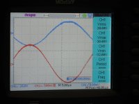
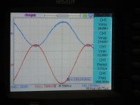
Then I saw in the pictures that the Transistor was running out of Phase by 180 Degrees, and this on all Frequencies.
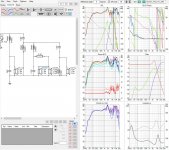
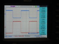
So today, I soldered it back into the PCB, but this time the right way.
Set up my Instruments and tuned to 1KHZ sine Wave 50% output. first thing I saw, was lots of Parasitic Noise, two small Capacitors together 33 and 22 Pico and the wave was just as beautiful as last night.
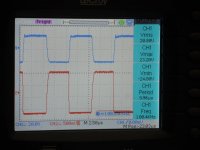
I do always search for the max, so Pictures are taken @20.8 volt, where the Wave starts to clip. Sine 500K is 16Volts RMS, still within 2db without clip.
But the follow up was not that nice anymore. 1Khz to 50KHz 20Volts RMS before Clipping, with shunt resistor of 1KOhm to GND.
Above that just Catastrophic. 100KHZ -1db 120 - 2db no way to get higher than 150K would output only 16Volts RMS. Still good but not to compare with last night.
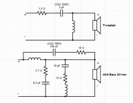
The BD139-10 pin layout is 1= Emitter 2= Collector 3= Base if seen from front where the label is printed. I soldered it with the label to the back, this would mean that E & B were reversed. So how the AMP POSSIBLE COULD work and WORK BETTER THAN when connected the RIGHT WAY.
Has anyone see something similar to this,??
Of course I have pics and I also will place the Circuit. But what you would say just out of the blue has happen. I tried to simulate that today on my computer, yea I could simulate it but with lost of distortion measured in the simulator software, but in real-time there wasn't any distortion.
Does anyone has an Idea,? Shall i put the Transistor the wrong way in to get better number? And after all the world would laugh at me, what a fool..
Thanks for any Input
Regards
Chris Hess
Look at the pics from Last night first. these from today
I will place later..


![700_432vr20[2].jpg](https://www.hifi-punkten.se/assets/uploads/products/1100/700_432vr20[2].jpg)


