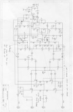
Hi Folks, first post from a relative newbie and former lurker, so here goes...hope you can read the circuit....its long, bear with me.
I am actually a switch mode PSU designer who moved into analogue and mixed signal semiconductor sales... it pays more!My background is Linear Tech, Burr Brown, Unitrode, TI but I have always had a hobby of audio dating back to when I was 11 years old...a long time ago now. Now I am selling motors..more on that another day.
I first experimented with nested feedback by putting a 400W MOSFET amp inside the feedback loop of a OPA627. Fixes the DC drift just great...and actually works quite well. Why...the sales director wanted 'more bass'. I reckon he just needed to clean out his ears...
But it got me interested in nested feedback, and I read the Cherry papers. And wished I could remember more of the stuff I learned at college.....that's what sales does to you.
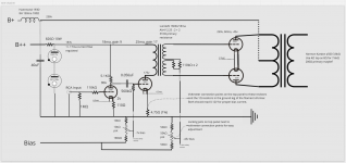
The original objective was, using the Cherry paper (with his permission for hobbist use incidentally), duplicate his results and make a judgement as to the subjective audio quality.
As time went on the project slowly mutated into a 'make it as best you can' then apply NDFL feedback.
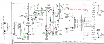
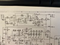
The input stage was elaborated to a CFP type in an attempt to achieve best linearity with the minimum additional complication.
The Rush stage was retained but with the inclusion of R21 to limit the maximum stage gain to something sensible...I am a pom after all so good to have a UK circuit in a Monash Univ. paper!
The VAS transistor was chosen as a BF469, to preserve as much HF performance as possible, rather than use a MJE. I appreciate other much better (and easier to obtain) transistors exist now.
Likewise the current source for the VAS stage was elaborated to a cascode. Later this was found very handy as it was modified to dethump the amp at turn on and diodes were added to the supply rails to prevent positive feedback thumping the amp at turn off.
The output stage was eleaborated into a CFP driver with common emitter output. The object here was to present minimal loading to the VAS, maxmimised voltage swing and allow multiple pairs of output devices to be driven, if a high power version was required.
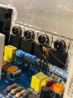
The prototype used Rod Elliots P03A as the driver...thanks Rod!
The output and driver transistors are the newish On Semi MJE15035 and 36 with MJL4XXX outputs.
The thermal tracking is split into two, one Vbe multiplier tracking the driver drift, the other tracking only the output temperature mounted smack on the face of the output transistor. This appears to work very well.
In the Cherry paper he suggests that including the output stage withn the CDOM loop is acceptable, it is certainly not using this more elaborate and possibly slower output stage, hence the position of C9 is conventional except that it is now part of a nested system.
The choice of transistors is not totally trivial in this design BTW, quite a lot of work was undertaken to prove the CFP stages were stable.
What does it sound like...well I think pretty good, no transistor 'edge' and very good resolution. It has powerful
but uncoloured bass too.
BTW some years ago I built the Self amps and verified his results..yes he's right THD+N circa <0.0005 in a 80KHz BW (APS1 noise floor stuff) but the amps sound diabolical on music, still have the pcbs if anyone interested. For anyone trying this, wiring up the amps and the test equipment is more critical than the choice of transistors...back to the Cherry amp..
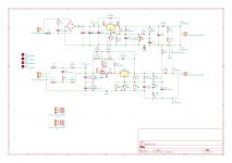
Spice analysis (thanks LTC, great free tool!) shows the overall loop gain to be very similar to an amplifier with 2 pole CDOM feedback, very high gain at low frequency, followed by a 2 pole roll off reducing to a single pole at unity. But this is achieved in a more controlled fashion, so I suspect, but cannot prove, lower overall distortion.
What do you guys out there in DIY land think?
😀 or

And thanks to Hugh Dean for tea and sympathy...sympathy for trying to build this thing in the first place!


 I want opinion on how to damp the outer side of the horns...


