Folks,
Over in the other meta thread we have been discussing the TDA1541.
https://www.diyaudio.com/community/threads/building-the-ultimate-nos-dac-using-tda1541a.79452/
Based on my experiences, various articles and application notes and practical work by a number of peeps we now have a pretty decent understanding of the TDA1541 and what makes it really tick. Much of it is in line with my previous understanding, but where before I had many black boxes I now have a better feel for the internal circuits and the various implications.
In short:
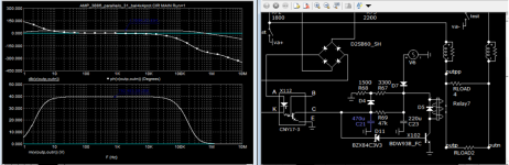
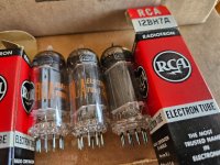
1) The TDA1541 needs a syncronised DEM system with correctly sized DEM filter capacitors and a way of feeding the DEM Oscillator pin's that do not cause DEM switching feed trough into the substrate. Empirically 8 X DEM Clocks (352.6/384kHz) offer the best objective performance.
Very low frequency DEM oscillators with big value electrolytic capacitors are an alternative but a bit questionable insofar as it takes hours of the DAC running to get to correct operation and long term stability is highly questionable. In the end both achieve the same fundamental result in different ways.
2) The TDA1541 has significant capacitive feedthrough from the digital inputs into the substrate and from there into the outputs. It is best imagined as a coupling capacitor of ~ 12pF between each digital input and the analogue outputs. 12pF does not sound like much but with MHz bit clock frequencies there is a lot of feedthrough.
Slowing down the edges of the input signals will reduce this. By using "Simultaneous Mode" we can lower the Bit Clock frequency maximally. At 192kHz Sample Rate we only have 3.072MHz Bit clock in this case. It means the edges can be slowed down much more without ill effects on the digital side, compared to I2S mode which typically has 12.288MHz Bit clock at 192kHz.
Existing "SIM" converters unfortunately (almost) all use the fallacious "stopped clock" system, which maximises the clock speed so a lot of clock feedthrough happens for a short duration and then nothing for the rest. This means we cannot slow down BCK edges too much, nor any others. So I will not consider such systems desirable.
There are debates around analogue stages and other TDA1541 related circuitry, but they are not (yet?) part of this project.
So, what is the project?
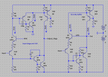
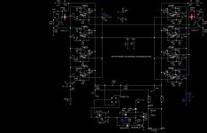
Make a PCB design (open sauce, free as in Free Speech and Free Beer) for a TDA1541(A) frontend that accepts an Amanero standard USB Module, incorporates an SPDIF receiver (optical, Coax and XLR) and includes an IIS to Simultaneous converter that outputs a continuous BCK at 16 X FS and the necessary LE Signal and Data and slew rate and voltage swing limiter circuitry.
Just add a TDA1541 (we might bring the IC position onto the PCB with other bits, this remains to be seen), power and analogue stage (where nobody seems to agree on anything).
As this is DIY Audio, we want to do this in discrete logic, not using CPLD or FPGA or bought in CPLD/FPGA Modules. Why no complex logic? Typically we find a few 100pS P-P additive Jitter from CPLD, FPGA or CPU's (e.g. XMOS). Ground bounce and other problems are significant. The IC cases are distinctly DIY unfriendly, a tool chain and programmer is also needed. It adds up. We can reclock to block a lot of this, but still, why?
With an Amanero Footprint (we can add more) the USB input is taken care of. For SPDIF the WM8804/05 series is EOL and others re unclear. So adding a CS8412(14) footprint is probably easiest, we can add suitable adapter PCB's for WM8804, CS8416/DP7416, AK4118 etc. on the PCB.
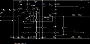
The main challenge is that we need to take a BCK of 64 X FS and a 2 X 32 Bit Data steam on one data line and output a BCK that is divided by 4 and two Data lines that have 16 Bit Per sample.
There are a number of possible approaches using shift registers, but as we need an input register to hold data from the I2S input (say 8 X 74HC595) and then an output register (say 4 X 74HC165) to hold 16 Bit that go to the TDA1541, this rapidly becomes a logic IC grave. We can find some 16 Bit Shift registers but these still account for a lot of circuitry.
On the plus side, the logic in this case becomes very transparent, obvious and easy to design and debug. Still 16 IC's or so seem a lot to me. It does remain an option.
An alternative would be to use the 74HC(T)40105 FIFO. As we have separate input and output clocks and the "elastic" FIFI we can stuff our 16 Bit into the Input side at the 64 X BCK speed and clock our data out steadily at 16 X BCK and the FIFO takes care of everything.
This would use one 40105 FIFO configured as 64 Bit Delay line with data taps at 16/32/48 and 64 Bit's so we can have the input bit's for our FIFO arrive simultaneously.
Two more 40105 FIFO handle data build as a 32 Bit X 4 FIFO. We stuff bit's into the first FIFO from where the ripple immediately to the output. We then clock out using our 16 X FS BCK. On the input side we invert MSB and only pass actual 16 Data bits, stopped input clock to block off the rest.
I think the FIFO solution is by far more elegant. An option for a secondary PLL with VCXO (or a VCLCXO) can be designed in as well.
A discussion start is here:
https://www.diyaudio.com/community/...ac-using-tda1541a.79452/page-517#post-7939329
So, if anyone wants to join into the discussion and project, feel free.
Thor