PMA CFA - current feedback power amplifier with +/-25V to +/-55V dc supply range
Intro
This project has started in the beginning of 2016 for the reason that I was interested in a current feedback topology (CFA) behaviour. The current feedback concept is well described in Renesas company application notes. For those who are interested, I recommend to download the application notes that I have linked below. I could hardly say anything more.
https://www.renesas.cn/cn/zh/document/apn/an9420-current-feedback-amplifier-theory-and-applications
https://www.renesas.cn/cn/zh/docume...ersus-current-feedback-operational-amplifiers
The goal was to design a simple and robust amplifier that would be able to drive difficult loads, would be stable and would have balanced time and frequency domain characteristics. The lowest nonlinear distortion was not the design goal, just to keep it inaudible.
Another goal was to make it working with a wide range of power supply voltages, here namely from 2 x 25V to 2 x 55 V.
The amplifier, with working title ACCE3, has been reliably operated for years, without a single problem.
Circuit design
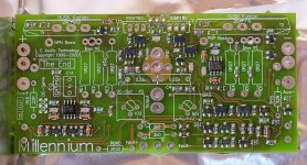
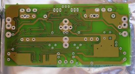
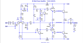
Amplifier schematics is as follows. The circuit is complete, with part numbers and values.
Q1-Q4 make a CFA input stage, with low impedance inverting input into R14/R15 common junction. Q5-Q8 make a VAS stage, with quite high current through Q5/Q6.
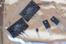
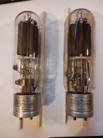
Output devices are 3 pairs of robust OnSemi MJL21194/93. Drivers are MJE15030/03. Similarly as in case of my PA4 amplifier, the rugged and reliable amplifier was my goal.
Supply voltage was tested at 2 x 25V and 2 x 55V, with no change in the circuit. The amplifier can easily drive 2 ohm load with 2 x 25V, staying completely safe. With 2 x 55V, I would recommend for the load impedance not to be lower than 3 ohm.
IC1, DC servo, is to be OPA177 opamp, for the reason of excellent DC parameters and for the reason of low idle current of 1.3 mA. This is necessary to cover wide supply range of 2 x 25V to 2 x 55V without unwanted high voltage drop across R32 and R33.
The amplifier is stable without an output coil, however, for safety reason I would recommend to add a parallel R//L combination 1uH//6R8 behind the X2-1 (X2-2) output terminal.
Construction notes
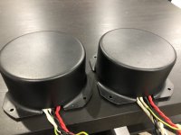
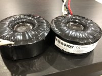
The amplifier is strictly dual-mono, channels do not share any common ground point, so no ground loops are created. The power supply has one transformer with separated secondary winding for left and right channel. It has separate center-tapped bridge rectifiers with capacitor banks of 2 x 14100 uF for each channel, as can be seen from the photos.
Voltage drop across 0R22 emitter resistors (R25 etc.) is set between 15mV - 22mV, which makes idle current per transistor equal to 68mA - 100mA.
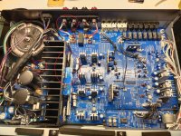
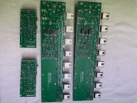
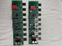
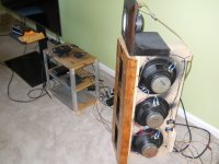
Photos of the amplifier
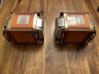
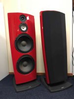
The amplifier with 2 x 25V dc supply built in my old Fischerelektronik 19” 3U 20+ years old prototype case can be seen below:

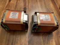
And this is the more detailed photo of one module built in another amplifier with 2 x 55V PSU.
 Basic specifications
•Output power 2 x 200W/4ohm with 2 x 55V supply, 2 x 40W/4ohm with 2 x 25V supply, THD 1%
•Frequency roll off (-3dB) 225kHz
•Harmonic distortion <0,02%/1kHz/100W/4ohm (2 x 55V PSU)
•CCIF 19kHz+20kHz 0,01%/30W/4ohm (2 x 55V PSU)
•Rise time of step response 1.4us
•Gain 27dB
•S/N ratio 94dB/2,83V/BW20kHz/linear, 114dB at full swing (2 x 55V PSU)
•minimum load impedance 2 ohm resistive/complex with 2 x 25V supply, 2 ohm resistive or 3 ohm complex with 2 x 55V supply
Measurements
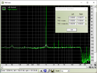
Amplitude and phase response within 20Hz – 40kHz range

We can see gain of 27.1dB and amplitude and phase response flat in the audio band.
Step response

Rise time (10% - 90%) of the step response is 1.28us when measured with the fast function generator with 10ns rise time. This indicates to 273kHz/-3dB amplifier bandwith.
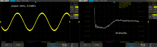
Response to 10kHz square

Response to square wave does not depend on signal amplitude, it is level invariant, thanks to CFA topology. This was measured with a generator with about 2 us rise and fall time.
Distortion measurements with 2 x 25V supply
THD+N vs. power at 1kHz into 4ohm load

I do not have an autoranger, so this was measured with 2 settings of ADC input range, 10V and 60V. This is for the reason that at 60V range the system noise is higher than amplifier noise and thus we get too high THD+N numbers at low power, due to measuring system intrinsic noise.
We can see that THD = 1% is at 40W and that the distortion knee is about 27W.
Comparison of THD+N vs. power at 1kHz into 2.2 ohm and 4 ohm load (and comparison of measurement vs. simulation)
measurement

simulation

THD+N = 1% is at 40W/4ohm and 60W/2.2ohm. There is no extreme rise of distortion into 2.2ohm load, the amplifier has no problem with it. And as always, simulated result is more optimistic than the real life result.
THD vs. frequency at 30W into 2.2ohm load

Distortion stays below 0.1% up to 22kHz. Below 100Hz we can see effect of heavy power supply load (ripple) due to high load current.
19+20kHz CCIF IMD
 Overload recovery according to IEC60286-3 (overload recovery time)
First. the definition. I find this test extremely important!
and, the measurements with 20Hz and 1kHz signals

 Distortion measurements with 2 x 55V supply

Measurements with 2 x 55V supply were done 4 and more years ago, with another measuring system, that was unable to make stepped THD and THD+N vs. power measurements properly. Please let me show only 100W/4ohm/1kHz spectrum.
Conclusion
The amplifier has proven to be reliable in operation since 2016. It is robust and able to drive difficult loads, while tested into complex load and R//C load.
https://pmacura.cz/pmacfa.htm
_____________________________________________________________________________________________________________________________________________________
Edit: Gerber files and BOM
I am attaching Gerber files and BOM which applies to the amplifier shown in the photos above and which were used for PCB production. Please note there is one wire jumper on the PCB shown in the pdf brd file. Gerber files updated with vertical power transistor packages!


 Translation: