You are using an out of date browser. It may not display this or other websites correctly.
You should upgrade or use an alternative browser.
You should upgrade or use an alternative browser.
Filters
Show only:
Bias issue
- Solid State
- 7 Replies
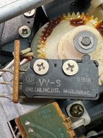
So working with brand new amplifier big and famous that had a customer complain about sound
initial test proved the amp was too cold
Checked bias according to the manufacturer and found low ....
Manufacturer need 8mv per transistor but found only 2.5
So adjusted bias and all appears to work fine .....
Placed a question to the chief engineer ( Turkish ) ( ?????? ) about it, since this is not only famous but also very expensive amp
And the answer was that may be from transportation trimmers have been moved Trimmers areBB top quality 10
 turn
turn
Please comment your opinion for this bellow
initial test proved the amp was too cold
Checked bias according to the manufacturer and found low ....
Manufacturer need 8mv per transistor but found only 2.5
So adjusted bias and all appears to work fine .....
Placed a question to the chief engineer ( Turkish ) ( ?????? ) about it, since this is not only famous but also very expensive amp
And the answer was that may be from transportation trimmers have been moved Trimmers areBB top quality 10
Please comment your opinion for this bellow
Differential inputs - diff all the way to ADC or convert to SE?
- By ckocagil
- Analog Line Level
- 3 Replies
I've been looking at the designs of some popular audio interfaces and I found that none of them contain in-amps (or even diff-amps) for their differential inputs. Instead they separately buffer the plus and minus inputs, route them through some analog switches and gain/attenuation circuitry, then to separate drivers for the differential ADC.
This was not the structure I expected! The ADC (CS4272) likes symmetric signals, so I'd rather have the input stage to immediately convert the diff inputs to single-ended with high CMRR instead of relying on the ADC. Sure, there's not much common-mode DC since the inputs are AC coupled with caps, but what about mains hum and other AC common-mode noise?
Is this for saving cost? Perhaps going diff->SE->diff would require 1-2 more op-amps.
Technics RSM-255X tape head source
- Analogue Source
- 7 Replies
I have an old Technics RSM 255X tape deck that works pretty good. I want to copy off some recordings I made with the dbx circuitry. It has some pretty outrageous hiss which may be due to the tape head wearing out, there is a definite groove on the surface. Does anyone know of a replacement or a source of parts. I could buy another on ebay but it probably has the same issue.
Substitute in Parasound 2SC3423-O or 2SC3423-Y and 2SA1360-O or 2SA1360-Y for unavailable 2SC3423/2SA1360 ?
- Parts
- 2 Replies
I'm wanting to replace 2SC3423 and complimentary 2SA1360 in a Parasound input stage (with a somewhat random oscillatory symptom). They seem to no longer be available but 2SC3423-O, 2SC3423-Y are, as are
I've read this "The 2SC3423 transistor can have a current gain of 80 to 240. The gain of the 2SC3423-O will be in the range from 80 to 160, for the 2SC3423-Y it will be in the range from 120 to 240."
Similarly, I've read "The 2SA1360 transistor can have a current gain of 80 to 240. The gain of the 2SA1360-O will be in the range from 80 to 160, for the 2SA1360-Y it will be in the range from 120 to 240."
Would these be plug'n play substitutes? The target circuit is shown in the attached pic.
Should other substitutes be considered instead?
Attachments

Hello from San Francisco
- By tapesnmoire
- Introductions
- 3 Replies
Hello,
I have worked in the hi-fi world for over six years now, and have performed and recorded music with samplers and synthesizers for closer to ten. Generally interested in all types of audio tech and good sound, although I was educated in the arts/humanities rather than engineering.
Maybe the first online forum I've joined ever. Happy to be part of what seems like a friendly and generous group.

Please take me to school on audible quality differences between capacitors, inductors, and resistors
As the title insinuates I need some lessons on the difference between cap, inductors, and resistors.
I know quite a bit about circuits but I always just grab whatever spec part I happen to need off of digikey when I need something.
I see things listed as "audio grade" which I assume to be total BS considering "audio grade" resistors are only 5%ers. I can get a better resistors for $1.50 at 1% from digikey.
Couples things I do not know is what the different is between caps. For example, the difference between a non polar one and a polar one. Is one better?
The difference between the inductors I also do not know. For example, is there an audible quality difference between an air core, copper foil, or iron core inductors?
If anyone can take me school on the specifics of these differences I am all ears because I really do not know.
Using IRF3205 instead of IRFP064N ???
Hi everyone,
I’m repairing a class D 3000W RMS amplifier, which uses a total of 12 IRFP064Ns in its power supply section. They are pretty hard to come by where I live. Can I use IRF3205 instead of them?
They look pretty similar on the datasheets, except for the safe operating areas.
I’m repairing a class D 3000W RMS amplifier, which uses a total of 12 IRFP064Ns in its power supply section. They are pretty hard to come by where I live. Can I use IRF3205 instead of them?
They look pretty similar on the datasheets, except for the safe operating areas.
Re-use an old box
- By invacuo
- Full Range
- 8 Replies
Hi,
I have an old 3 way old loudspeaker with missed bass driver. I cannot get same driver because in no longer available. Can I install a new bass driver and try to adjust the bass reflex port? Is that possible?.
Thanks for your help.
Regards.
I have an old 3 way old loudspeaker with missed bass driver. I cannot get same driver because in no longer available. Can I install a new bass driver and try to adjust the bass reflex port? Is that possible?.
Thanks for your help.
Regards.
Hello
- By aliaksand
- Introductions
- 1 Replies
Hello. I'm new to this forum. My work is related to the repair of electronic equipment in the field of welding. My hobby is audio engineering. I was interested in one of the forum's projects, that's why I'm here.
Custom audio transformers - input, DAC/MC, interstage, output
- By Dorin Bodea
- Vendor's Bazaar
- 4 Replies
Just in case you need a custom audio transformer like the one in attach you can contact me and if it's doable then you can have what you won't find in other places.
I use mainly mumetal/permalloy and HiB/GOSS and you can see some results in the FB page attached, where I list from time to time some of my projects, you don't need an account.
https://www.facebook.com/profile.php?id=100057288107123

I'm located in Europe, but in the last 20 years I've sent my xfmrs pretty much all aver the world 🙂
I use mainly mumetal/permalloy and HiB/GOSS and you can see some results in the FB page attached, where I list from time to time some of my projects, you don't need an account.
https://www.facebook.com/profile.php?id=100057288107123
I'm located in Europe, but in the last 20 years I've sent my xfmrs pretty much all aver the world 🙂
Hello from Argentina
- By matcarfer
- Introductions
- 1 Replies
Hello everyone. New to the forum but been studing Volumio vs Daphile for a while.
Got a nice USB DAC and found that Tidal support is suscription based on Volumio so I discarded it. Will use Daphile.
I plan to use Daphile for all my music needs. Sadly, I have a really low power pc (Atom X5 with 2GB RAM) with an USB DAC, so I can't figure out if REALTIME KERNEL is better or worse, and in which case I use it (or not). Not even the official website, faq or readme says anything about it, and I can't seem to find any official forum or place to chat/discuss about Daphile save for THIS thread. Help!
THREAD:
https://www.diyaudio.com/community/threads/daphile-audiophile-music-server-player-os.240040/
Go Play problem
- By The Painter
- Construction Tips
- 21 Replies
I have just purchased a Harmon Kardon Go Play from a local charity shop. This is the very early model and I was told that it worked and for £25 I thought that I would "Suck it up" if I found a problem. Yes I found that one Channel had low level distortion! When playing loud and upsetting my upstairs neighbours it was hardly noticeable, but I like lowish levels of sound. Before my NOVICE hands do any further damage and it go's in the frustration bin, can some kind soul plot a path to fault find this problem! Many thank's.
DaytonAudio SPA500 hum/buzz
- By BunBun
- Solid State
- 2 Replies
I have a SPA500 powering a CSS 12" sub. Hanging the plate amp off the back of the sub enclosure. Built this sub back in 2016, has worked great until I moved it from my work office to my home office. It got jostled around quite a bit moving it down my stairs and when I plugged it in immediately this loud buzzing I associate with mains (60Hz) comes through the woofer. After checking all the wires and changing power sources I gave up but came back to it later and it was dead silent. Turns out after awhile it sorts itself out and as long as I didn't unplug the amp it was fine. Ie. waking up from auto power off wouldn't result in the buzz/hum.
However, now a few weeks later it's making a slight buzz when coming out of auto off that isn't as loud as when it's from pull power disconnect state but it also doesn't fully go away anymore. I assume whatever the issue is, is getting worse.
Anyone have any advice they can share of how I can troubleshoot which component(s) I need to replace? The amp appears to work fine otherwise and the price on these amps has skyrocketed since I last purchased so I would like to try a repair myself. I am fully capable of using electronics diagnostic equipment though I do not have an oscilloscope. I've built and repair several electronic kits and devices in the past I have no issues doing solder rework on a device like this. I just don't know much about analog amp design or diagnostics.
2 Full range speakers + 1 subwoofer for monitoring system in DJ desk
- By cioz
- Full Range
- 23 Replies
Hi! I want to build a DJ desk for my living room, and I want to integrate 2 full range speakers in the desk (left and right, at 45 degree, tilted at 45 degree towards the top: almost studio vibe) plus 1 subwoofer under the desk. So when you move the desk the whole system is moving with it.
I couldn’t find projects like this online (maybe I haven’t searched enough) so I was wondering if it does make sense at all or not.
If it does, I wanted to ask: which kind of full range driver would you recommend for monitoring? I wanted something that would reach at least 90hz, with a SPL at 1m of minimum 88db and I found a coaxial speaker from Dayton that would work good, but I never tried it.
https://www.soundimports.eu/en/dayton-audio-cx120-8.html
These could reach 80hz when ported. But I ask myself. Does it make sense to make them ported if I use a subwoofer?
I would pair them with this subwoofer:
https://www.soundimports.eu/en/grs-8sw-4he-8.html
Is it good to go for these coaxial speaker? Should I go vented or not for the full range speakers? Would you recommend something else instead?
I would like to avoid building crossovers, and go one way.
I hope somebody can give me some ideas ❤️
Thank you in advance!
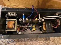
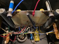
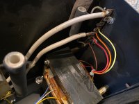
A & R Cambridge A60 Intergrated amp
- By Meerkat 70
- Solid State
- 11 Replies
A fellow member of the website Canuck Audio asked me to have a look at this amp, it blew the power fuse along with the 3 amp fuses on the power rails.
I replaced the power fuse and removed the rail fuses and the unit does power up, at least the power supply is okay. Trying fuses in the power rails makes the dim bulb tester light up full brilliance indicating a short. I read a bit about these amps and they seem to burn fuses and output transistors galore.
I tried testing the output transistors in circuit and they seem okay, I will need to remove the whole circuit board, only thing is I need to remove the knobs and I do not have an allen key that fits the small screw.. Are they unique or just British? Anyone know the size, none of mine fit.
Any tricks to check this amp out, it seems well built with good components. Appreciate any help if you have done repairs on this amp.
Thanks Wayne
Pure Tube i/V for ES9038PRO-9028, 9018, AKM...
- By quanghao
- Group Buys
- 114 Replies
Hello all friends!
After many years of using ES chips, we have experienced with DAC, ES9018S, ES9038PRO.
We are glad to announce to you that we have succeeded in designing the output for ES9038PRO, undergoing over 15 different designs, we chose the best design to share for you. Yes, you can make yourself a DAC with pure tube output.
I call it: Pure Tube i / V balanced.
Andrea-Quanghao-Morten would like to share our design with you!
Sincerely thank you.
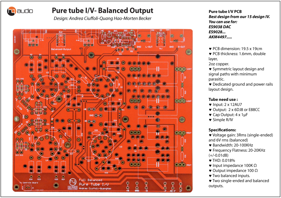
1. Pure tube I/V- Balanced Output
Pure tube I/V PCB
Best design from our 15 design IV.
You can use for:
ES9038 DAC
ES9028...
AKM4497.....
♥ PCB dimension: 19.5 x 19cm
♥ PCB thickness: 1.6mm, double layer,
2oz copper.
♥ Symmetric layout design and signal paths with minimum
parasitic.
♥ Dedicated ground and power rails layout design.
Tube need use :
♥ Input: 2 x 12AU7
♥ Output: 2 x 6DJ8 or E88CC
♥ Cap Output: 4 x 1µF
♥ Simple R/IV
price: 45$
EX:
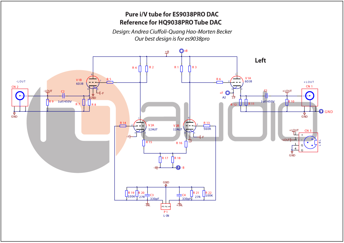
And Pure i/V schematic L:
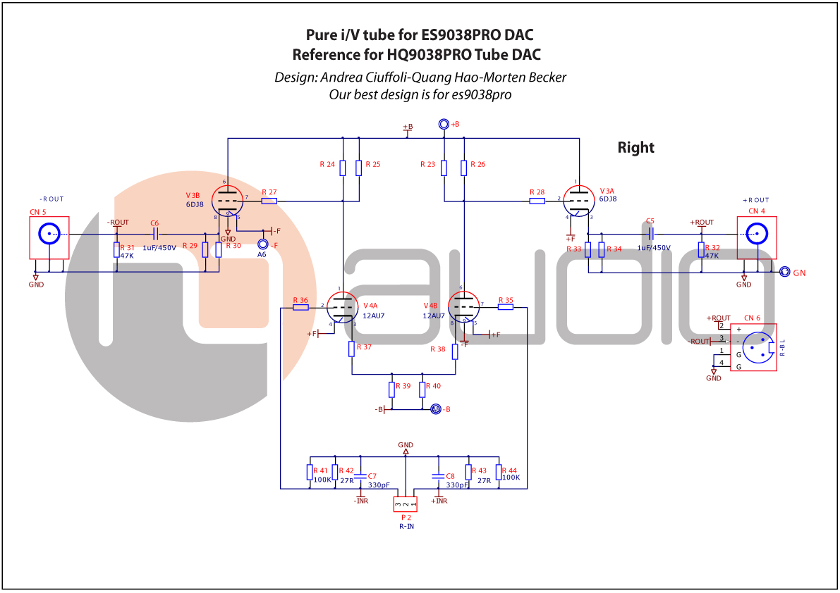
And Pure i/V schematic R:
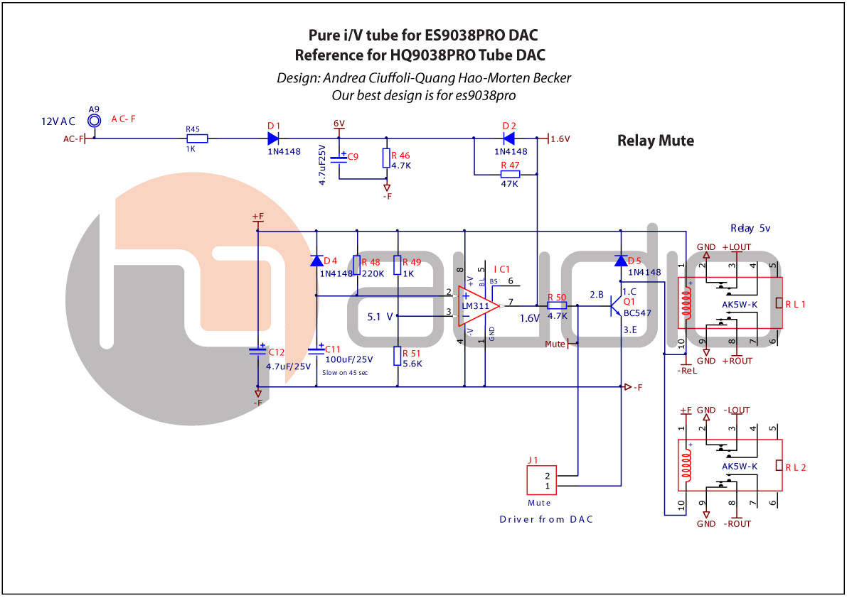
And Pure i/V schematic Relay:
2. HQ-Hv Supply for Tube IV
Output:
1. Positive voltage:
♥ 100-270VDC.
2. Negative voltage:
♥ 100-270VDC.
♥ Low noise , Low Z-out
♥ Use mosfet
3. Filemant Tube: 6.3VDC
to 12VDC/3A.
price: 35$
And Hq-hv schematic:
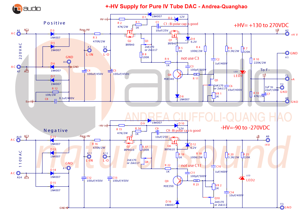
And schematic Filemant

Shipping by transport envelope for all countryll contry: 25$.
Payment by paypal: quanghao168@yahoo.com.vn
Paypal free: 2%.
After many years of using ES chips, we have experienced with DAC, ES9018S, ES9038PRO.
We are glad to announce to you that we have succeeded in designing the output for ES9038PRO, undergoing over 15 different designs, we chose the best design to share for you. Yes, you can make yourself a DAC with pure tube output.
I call it: Pure Tube i / V balanced.
Andrea-Quanghao-Morten would like to share our design with you!
Sincerely thank you.
1. Pure tube I/V- Balanced Output
Pure tube I/V PCB
Best design from our 15 design IV.
You can use for:
ES9038 DAC
ES9028...
AKM4497.....
♥ PCB dimension: 19.5 x 19cm
♥ PCB thickness: 1.6mm, double layer,
2oz copper.
♥ Symmetric layout design and signal paths with minimum
parasitic.
♥ Dedicated ground and power rails layout design.
Tube need use :
♥ Input: 2 x 12AU7
♥ Output: 2 x 6DJ8 or E88CC
♥ Cap Output: 4 x 1µF
♥ Simple R/IV
price: 45$
EX:
And Pure i/V schematic L:
And Pure i/V schematic R:
And Pure i/V schematic Relay:
2. HQ-Hv Supply for Tube IV
Output:
1. Positive voltage:
♥ 100-270VDC.
2. Negative voltage:
♥ 100-270VDC.
♥ Low noise , Low Z-out
♥ Use mosfet
3. Filemant Tube: 6.3VDC
to 12VDC/3A.
price: 35$
And Hq-hv schematic:
And schematic Filemant
Shipping by transport envelope for all countryll contry: 25$.
Payment by paypal: quanghao168@yahoo.com.vn
Paypal free: 2%.
Audio Alchemy DDS-PRO Transport
- By Redwingnine
- Digital Source
- 51 Replies
I recently picked up a Audio Alchemy DIT Pro 32 and DDS 3.0 DAC. I picked this up for use in a second system. The sound from this pair is quite nice, somewhat better than I would have thought.
I'm considering looking for a DDS PRO Transport, as I wish to take advantage of the I2S output to the DTI. Using the I2S from the DTI to the DDS did provide a noticeable improvement over BNC.
So, a couple of questions: 1) Are there replacement parts for DDS PRO available, and, 2) Are there other transports that support the I2S out?
Hi
- By FunOrOff
- Introductions
- 1 Replies
Hey,
I'm a lover of both old-school sound and the practicality of modern technology, that's where the diy part will come in handy!
I'm a lover of both old-school sound and the practicality of modern technology, that's where the diy part will come in handy!
DSP amplifier required
Hi, I have a Behringer NX1000D for home use, and would like to replace it with something better. I use the DSP to EQ the speakers and room, and the one feature that I can’t find on many DSPs is DEQ. This is like a normal parametric equaliser, but with its own compressor. I have a 70Hz notch on the left speaker due to a bay window, and fill this in with the right speaker. This needs +8dB, so having a compressor on this stops overdriving anything when it’s loud, and there’s usually beer involved when it’s loud, so no one notices the notch
Any suggestions please on something around 50W per channel, and a bit more hi-fi and less PA. Thanks
Brian
PS Couldn’t find a better section to post it in, but open to any amplifier technology, class AB etc
Any suggestions please on something around 50W per channel, and a bit more hi-fi and less PA. Thanks
Brian
PS Couldn’t find a better section to post it in, but open to any amplifier technology, class AB etc
"The (Barrie) Gilbert Paper" "Are OP Amps Really Linear"
- By PB2
- Solid State
- 6 Replies
We discussed this paper over a decade ago and it was online at the time but, today, I had to use the Wayback Machine
to find it. Making it a thread here so that it is not lost forever. I believe that there was also a .pdf of it. Most of the
theory also applies to power amps.
There are a few Figures that were not captured.
A few very old links where it was discussed:
This one is almost 20 years old:
https://www.diyaudio.com/community/...rning-cordell-otala-and-gilbert-papers.48873/
Fairly certain that it was referenced here also, not saying that this is a good thread but here it is:
https://www.diyaudio.com/community/threads/whats-your-reasoning-and-not-whats-your-belief.41770/
Everyone knows that op amps are the most linear building blocks in the analog repertoire. If you want nonlinear behavior, you had better look to multipliers or other arcania. But we recognize that every real amplifier has a bit of nonlinearity, like it or lump it, so maybe we ought to take a look at just how good is that standard op amp, the voltage-mode amplifier identified as an 'OPA' in previous columns, when used at frequencies above a few Hertz.
It wasn't so many years ago, in the heyday of the uA741, that a guy called Otala discovered this early 1-MHz OPA performed a lot worse than might expected at audio frequencies, so he wrote a paper in the Journal of the Audio Engineering Society in which he coined a brand new term -- transient intermodulation distortion, or 'TIM' -- to describe in audio lingo what most users of op amps had already discovered, namely, the little matter of a limited slew-rate. It was a phenomenon peculiar to IC op amps. If you had grown up with vacuum tubes, you had plenty of reason to raise your eyebrows, since, unlike bipolar transistors (with their extremely high gm and a correspondingly small range over which linearity prevails in the familiar differential-pair gain cell), tube amplifiers rarely, if ever, got themselves into this pathological state of affairs.
Predictably, Otala's 'discovery' only added welcome fuel to the fire of those who were quite convinced that these new-fangled transistor amplifiers were genetically incapable of pleasing the audiophile ear, a notion which, like all myths, persists unabated, in spite of the fact that the root cause of TIM is now completely understood, and can easily be avoided in transistor amplifiers expressly designed for the most demanding audio applications. Nevertheless, Mister Otala was on to something, and although there are many splendid op amps out there, not all deliver quite what the textbooks promise. Accordingly, for a few minutes, we will examine a major source of distortion in op amps. Writing this in Kailua-Kona, Hawaii, with the thunder of the surf just feet away from this lanai, as the palms and hibiscus breathe the balmy post-dawn air, I have ample time on my hands.
The dominant mantra intoned over the application of op amps goes something like this: Never mind what's inside that cute little triangle; the function of the overall linear block -- invariably just a simple amplifier or filter stage -- is determined (almost entirely) by the passive components that are added to provide feedback. The triangle thing is merely the power-house that, come rain or shine, makes everything work out right in the end, by a kind of op-amp magic. The parenthetical inclusion is a concession to those who know a bit better, and it's the focus of this piece.
Reduced to essentials, most voltage-mode op amps, OPAs, are based on a topology like that shown in Fig. 1. To develop the theory, our device is here connected as a simple amplifier with a closed-loop gain of G, determined by the ratio (R1+R2)/R2, which can alternatively be expressed in terms of the feedback fraction b = 1/G. Because the dominant source of nonlinearity is in the input cell, the distortion will be lowest in the voltage-follower mode.
In the interests of clarity and analytical simplicity, we will assume here that the output is a perfect sinusoid, having an amplitude E and angular frequency w, that is, Esinwt, and work backwards from this output to deduce what VIN would need to be to generate that output. This may seem an odd approach, and it's certainly not essential to do it this way. However, many analyses involving the exponential behavior of transistors lead to transcendental solutions when pursued in the forward direction, and that's true in this case. A reverse-direction analysis quickly generates the key insights, and points towards the required modifications to effect a solution, at the price of a slight but not serious loss of rigor.
A bipolar implementation is shown, since many monolithic OPAs use this technology. A basic differential-pair Q1, Q2, also cast in pnp form, and having a near-perfect current-source IT in its 'tail', senses the difference between the applied input VIN and some fraction of the output, while being insensitive to common-mode levels. In the case of a voltage follower, of course, the distinction between the signal and the common-mode voltage is somewhat fuzzy; the real value of the high common-mode rejection ratio (CMRR) afforded by OPAs is much more apparent when the amplifier is connected in a high-gain mode, and a small input signal is accompanied by an interfering common-mode signal.
Formally, this input cell is a nonlinear transconductance, whose output currents IC1 and IC2 are applied to the npn current-mirror Q3, Q4, which generates the difference IC1 - IC2. This current is then integrated by the 'HF compensation' capacitor, CC, in the main voltage-gain stage provided by the common-emitter stage Q5, which is forced to operate at a constant collector current of IT. The resulting output voltage is buffered by what is here shown as an ideal voltage-controlled voltage-source (VCVS) but which in most cases will be the familiar Class-AB complementary emitter-follower that provides the high current-gain to drive the load, RL.
In a real OPA, some of the open-loop distortion will arise in this VCVS stage, but in order to keep our sights focused on the main distortion mechanism, we can ignore that here. Notice that CC is connected to the final output node, not to the collector of Q5, as is often the case. This minor modification means that back-and-forth flow of the HF displacement current in CC is not supported by Q5 but, rather, by the output stage. Consequently, there is no variation in IC5 (it's held steady at IT) and thus the VBE of Q5 is likewise constant with output voltage.
All this groundwork may seem very tedious, but it is with a view to getting at the root cause of distortion. Numerous such detailed considerations are crucial to the design of an op amp capable of ultra-linear HF performance, and each needs to be eliminated independently. We're only considering the first of many, here.
Now we're ready to start the sums. Unfortunately, there is no painless way to avoid mathematics, but what we can do is use simple, even rudimentary, models for the transistors, in the spirit of Foundation Design. This approach to the quest for insight was mentioned in the "Spicing Up The Op Amp", and it's time to be a little more specific about this notion. It works very well for the bipolar junction transistor (BJT), which will probably remain a major technology -- certainly in the high-performance arena -- for at least the next decade, and beyond, in spite of the impressive advances in analog CMOS design, only made more difficult by the almost total emphasis on digital applications in the on-going development of sub-micron technologies. (Some of the reasons for holding to this view were stated in "Why Bipolar?".)
The Level-0 model for the BJT is simply a voltage-controlled current-source (VCCS) having an exact exponential relationship between its collector current, IC, and its base-emitter voltage, VBE; this is the heart of the BJT:
IC = IS exp (VBE/VT) (1)
where IS is the saturation current (and, only slightly whimsically, can be regarded as the BJT's soul, since it mediates so much of the device's personality) having a value of some 3.6E-18 amps for a VBE of 800 mV at IC = 100 mA and temperature of 27ıC. It's amazing to me, after having stared at this equation for the better part of my life, how very profound it is, traceable to fundamental aspects of carrier statistics in semiconductor materials. It is the well-spring of BJT magic. It takes but a moment to find that the transconductance dIC/dVBE of a single device is:
gm = IC/VT (2)
where VT is, of course, the thermal voltage kT/q, 26 mV at 30ıC. This remains as true for a modern complex SiGe heterojunction transistor as it was for the primitive junction-alloy devices that came along quite shortly after Bardeen, Brattain and Shockley went whooping up and down the halls of Bell Labs jubilantly shouting Eureka! It's fair to say that (1) and (2) are the most remarkable of all equations in modern electronics.
The Level-0 model also conveniently omits such pesky set-backs as the finite base current and Early voltage of a BJT, its ohmic resistances and parasitic capacitances, base transit time and other effects. Accordingly, we set BF = BR = VAF = VAR = 1E6, and most other parameters to zero. Crazy? Not really: This is just what first-order textbook analyses do, without drawing attention to the fact. It is nonetheless surprising just how much of the reality of an IC's behavior emerges from the application of this simple translinear model to circuit analysis. For example, the minimum permissible supply voltage will usually be correctly modeled; the shot noise will be right on the money; most of the temperature behavior; and, for the present purposes, an important distortion mechanism in OPAs will be quite accurately predicted.
to find it. Making it a thread here so that it is not lost forever. I believe that there was also a .pdf of it. Most of the
theory also applies to power amps.
There are a few Figures that were not captured.
A few very old links where it was discussed:
This one is almost 20 years old:
https://www.diyaudio.com/community/...rning-cordell-otala-and-gilbert-papers.48873/
Fairly certain that it was referenced here also, not saying that this is a good thread but here it is:
https://www.diyaudio.com/community/threads/whats-your-reasoning-and-not-whats-your-belief.41770/
Everyone knows that op amps are the most linear building blocks in the analog repertoire. If you want nonlinear behavior, you had better look to multipliers or other arcania. But we recognize that every real amplifier has a bit of nonlinearity, like it or lump it, so maybe we ought to take a look at just how good is that standard op amp, the voltage-mode amplifier identified as an 'OPA' in previous columns, when used at frequencies above a few Hertz.
It wasn't so many years ago, in the heyday of the uA741, that a guy called Otala discovered this early 1-MHz OPA performed a lot worse than might expected at audio frequencies, so he wrote a paper in the Journal of the Audio Engineering Society in which he coined a brand new term -- transient intermodulation distortion, or 'TIM' -- to describe in audio lingo what most users of op amps had already discovered, namely, the little matter of a limited slew-rate. It was a phenomenon peculiar to IC op amps. If you had grown up with vacuum tubes, you had plenty of reason to raise your eyebrows, since, unlike bipolar transistors (with their extremely high gm and a correspondingly small range over which linearity prevails in the familiar differential-pair gain cell), tube amplifiers rarely, if ever, got themselves into this pathological state of affairs.
Predictably, Otala's 'discovery' only added welcome fuel to the fire of those who were quite convinced that these new-fangled transistor amplifiers were genetically incapable of pleasing the audiophile ear, a notion which, like all myths, persists unabated, in spite of the fact that the root cause of TIM is now completely understood, and can easily be avoided in transistor amplifiers expressly designed for the most demanding audio applications. Nevertheless, Mister Otala was on to something, and although there are many splendid op amps out there, not all deliver quite what the textbooks promise. Accordingly, for a few minutes, we will examine a major source of distortion in op amps. Writing this in Kailua-Kona, Hawaii, with the thunder of the surf just feet away from this lanai, as the palms and hibiscus breathe the balmy post-dawn air, I have ample time on my hands.
The dominant mantra intoned over the application of op amps goes something like this: Never mind what's inside that cute little triangle; the function of the overall linear block -- invariably just a simple amplifier or filter stage -- is determined (almost entirely) by the passive components that are added to provide feedback. The triangle thing is merely the power-house that, come rain or shine, makes everything work out right in the end, by a kind of op-amp magic. The parenthetical inclusion is a concession to those who know a bit better, and it's the focus of this piece.
Reduced to essentials, most voltage-mode op amps, OPAs, are based on a topology like that shown in Fig. 1. To develop the theory, our device is here connected as a simple amplifier with a closed-loop gain of G, determined by the ratio (R1+R2)/R2, which can alternatively be expressed in terms of the feedback fraction b = 1/G. Because the dominant source of nonlinearity is in the input cell, the distortion will be lowest in the voltage-follower mode.
In the interests of clarity and analytical simplicity, we will assume here that the output is a perfect sinusoid, having an amplitude E and angular frequency w, that is, Esinwt, and work backwards from this output to deduce what VIN would need to be to generate that output. This may seem an odd approach, and it's certainly not essential to do it this way. However, many analyses involving the exponential behavior of transistors lead to transcendental solutions when pursued in the forward direction, and that's true in this case. A reverse-direction analysis quickly generates the key insights, and points towards the required modifications to effect a solution, at the price of a slight but not serious loss of rigor.
A bipolar implementation is shown, since many monolithic OPAs use this technology. A basic differential-pair Q1, Q2, also cast in pnp form, and having a near-perfect current-source IT in its 'tail', senses the difference between the applied input VIN and some fraction of the output, while being insensitive to common-mode levels. In the case of a voltage follower, of course, the distinction between the signal and the common-mode voltage is somewhat fuzzy; the real value of the high common-mode rejection ratio (CMRR) afforded by OPAs is much more apparent when the amplifier is connected in a high-gain mode, and a small input signal is accompanied by an interfering common-mode signal.

Formally, this input cell is a nonlinear transconductance, whose output currents IC1 and IC2 are applied to the npn current-mirror Q3, Q4, which generates the difference IC1 - IC2. This current is then integrated by the 'HF compensation' capacitor, CC, in the main voltage-gain stage provided by the common-emitter stage Q5, which is forced to operate at a constant collector current of IT. The resulting output voltage is buffered by what is here shown as an ideal voltage-controlled voltage-source (VCVS) but which in most cases will be the familiar Class-AB complementary emitter-follower that provides the high current-gain to drive the load, RL.
In a real OPA, some of the open-loop distortion will arise in this VCVS stage, but in order to keep our sights focused on the main distortion mechanism, we can ignore that here. Notice that CC is connected to the final output node, not to the collector of Q5, as is often the case. This minor modification means that back-and-forth flow of the HF displacement current in CC is not supported by Q5 but, rather, by the output stage. Consequently, there is no variation in IC5 (it's held steady at IT) and thus the VBE of Q5 is likewise constant with output voltage.
All this groundwork may seem very tedious, but it is with a view to getting at the root cause of distortion. Numerous such detailed considerations are crucial to the design of an op amp capable of ultra-linear HF performance, and each needs to be eliminated independently. We're only considering the first of many, here.
Now we're ready to start the sums. Unfortunately, there is no painless way to avoid mathematics, but what we can do is use simple, even rudimentary, models for the transistors, in the spirit of Foundation Design. This approach to the quest for insight was mentioned in the "Spicing Up The Op Amp", and it's time to be a little more specific about this notion. It works very well for the bipolar junction transistor (BJT), which will probably remain a major technology -- certainly in the high-performance arena -- for at least the next decade, and beyond, in spite of the impressive advances in analog CMOS design, only made more difficult by the almost total emphasis on digital applications in the on-going development of sub-micron technologies. (Some of the reasons for holding to this view were stated in "Why Bipolar?".)
The Level-0 model for the BJT is simply a voltage-controlled current-source (VCCS) having an exact exponential relationship between its collector current, IC, and its base-emitter voltage, VBE; this is the heart of the BJT:
IC = IS exp (VBE/VT) (1)
where IS is the saturation current (and, only slightly whimsically, can be regarded as the BJT's soul, since it mediates so much of the device's personality) having a value of some 3.6E-18 amps for a VBE of 800 mV at IC = 100 mA and temperature of 27ıC. It's amazing to me, after having stared at this equation for the better part of my life, how very profound it is, traceable to fundamental aspects of carrier statistics in semiconductor materials. It is the well-spring of BJT magic. It takes but a moment to find that the transconductance dIC/dVBE of a single device is:
gm = IC/VT (2)
where VT is, of course, the thermal voltage kT/q, 26 mV at 30ıC. This remains as true for a modern complex SiGe heterojunction transistor as it was for the primitive junction-alloy devices that came along quite shortly after Bardeen, Brattain and Shockley went whooping up and down the halls of Bell Labs jubilantly shouting Eureka! It's fair to say that (1) and (2) are the most remarkable of all equations in modern electronics.
The Level-0 model also conveniently omits such pesky set-backs as the finite base current and Early voltage of a BJT, its ohmic resistances and parasitic capacitances, base transit time and other effects. Accordingly, we set BF = BR = VAF = VAR = 1E6, and most other parameters to zero. Crazy? Not really: This is just what first-order textbook analyses do, without drawing attention to the fact. It is nonetheless surprising just how much of the reality of an IC's behavior emerges from the application of this simple translinear model to circuit analysis. For example, the minimum permissible supply voltage will usually be correctly modeled; the shot noise will be right on the money; most of the temperature behavior; and, for the present purposes, an important distortion mechanism in OPAs will be quite accurately predicted.
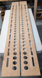
I wish I had a CNC router
- By Neil Davis
- Multi-Way
- 11 Replies
I hand to cut those ovals using my DIY flattening jig 🙁. And then spend several hours cleaning up the burn marks (cherry). But the front panel is finally ready to glue to the side panels. I still need to make 23 more tweeter assemblies. Fortunately, the 20-channel amp is done, although there is lots of code involved, which by definition is never done 🙂
Attachments
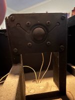
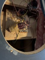
Acoustat MK-121-2A questions
- By techpurch
- Planars & Exotics
- 9 Replies
Based on these pics of my MK-121-2A, can anyone tell me if this is unmodified? Also, looking at the 3rd pic with the strip with options to connect to red, orange, and yellow wires, what are these options for? It is currently wired to the middle/orange tap.
Attachments

SSR01 and SSR02 super regulator group buy
- By peranders
- Group Buys
- 20 Replies
Just checking the interest for a group buy of my single channel regulators, SSR01 (positive output voltage) and SSR02 (negative output voltage).
The design has the following feature:
I will put up a google doc list for signing up interest. I will also come back with prices and conditions. The price will be good, I can assure you.
The design has the following feature:
- 4-layer pcb with 70 um (2 oz.) copper.
- Power traces 140 um!
- Gold pads.
- Extremely low noise.
- Extremely low output impedance in the audioband.
- Small size.
- Easy to change voltage, also to negative voltage but this particular design (pcb) requires two different pcb's, one for positive voltages and one for negative.
- Well-known and well-tested in serious and demanding applications.
- Option for TO92 or SOT23 transistors for the small signal transistors.
- Option for DIL08 or SO08 opamp.
- LM431 (and similar) reference or devices like LM329. The pcb has a universal footprint.
- Trimming options for both the reference and the feedback. Room for extra resistors and trimpots.
- One output with sense inputs.
- Option for using higher voltage than the max supply voltage for the opamp.
I will put up a google doc list for signing up interest. I will also come back with prices and conditions. The price will be good, I can assure you.
Attachments
4 large dual woofer speakers
I just picked up 4 of these dual woofer 3 way speakers. They were probably custom built in the 1970, they big and heavy. I've have been fixing the crossovers that fell apart over time.
The midrange and tweeters appear to be good quality and are mounted on top with speaker cloth covering the front and sides. The rear ported cabinets are approximal 3.3 cf with 2 10" woofers that I guess are Eminence. The internals have some unique braces and a quasi labyrinth design.
Any suggestions on how to get a better response curve?
Attachments

OEM Car Stereo modifications
- By Thatguy0213
- Electronic Design
- 1 Replies
Hello, I am like many people and looking for a way to retain my original radio system, specifically the way it looks. I have already looked into a lot of different things such as hideaway systems etc.
I want the OEM radio to control the sound system so after doing some basic math I have found one way that stands out to me, and would like feedback over feasibility and difficulty
Purchase a preexisting radio and put the components inside of my current OEM unit, then make the OEM buttons control the new radio/stereo.
The interface/faceplate on many new single din radios are detachable, which would allow me to solder either through that specific port or to the individual locations on the board.
The front of the radio I want to keep is from a 1996 F150 (16 buttons and a small display).
Would it be easier to use individual buttons, attempt to make a PCB or solder board, try to break down the current board and use it for the buttons? Also, is there something else that I am completely overlooking? Something easier?
I have a basic electrical background and understand a lot of the basic context that would be used here. Obviously a lot of it will be a learning opportunity as well, which I am excited for. So any help/guidance is appreciated.
3rd order low pass butterworth filter, correct calculations?
- By cristy6100
- Subwoofers
- 4 Replies
Hello and a good day to all, I am fairly new to crossover designs, I am trying to make a passive 3rd order butterworth crossovernfor my subwoofer, I have the following components:
L1 2.85mH ESR 0.15ohm ferrite bell core
C1 3 x 220uf bipolar caps for the shunt
L2 1.18mH ESR 0.2ohm same ferrite bell core inductor
The woofer has a Re of about 3.8ohms
I am trying to get close to about 150hz cutoff,
I did some calculations and I should be close to this value with the given components, but I am new to crossovers and maybe my calculations are wrong
Could anybody help me if these values will result in close to 150hz?
I can alter the capacitor to increase the value if needed, but I don't have larger value inductor
Thank you all for your time and help with this
Criss
Investing in Test equipment
- Equipment & Tools
- 25 Replies
I am looking to invest in some test lab equipment to enable accurate testing of circuits I build or modify. Ultimately I would like to be in a position a year from now to be able to diagnose audio amplifiers, tube and solid state and fix them.
Admittedly apart from college I have no electronic testing experience other than validation of test reports frequency plots etc.
So to summarise:
1.) If you could advise on educational resources that I could learn the theory from.
2.) Starting with an initial budget of say £2k, equipment that you would invest in and why.
3.) Initially I want to do this as a hobby but ultimately as a evening job diagnosing/ fixing audio equipment- in today's climate specifically in the UK is there much scope for this (no pun intended), or are the margins that small it's not viable as anything other than a hobby?
Your thoughts, feedback, advice, guidance are welcome.
Thanks
Paul
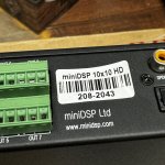
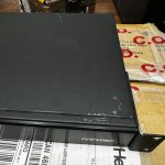
MiniDSP 10x10 HD
- By fireanimal
- Swap Meet
- 2 Replies
No issues other then a few scratches on top from rack mounting. 300 USD
Attachments

Hello
- By rfinck
- Introductions
- 2 Replies
Hi
my name is Rainer. I am following diya for more than 10 years but wasn't active to avoid matter of conflicts. For the last 30 years I was in various positions in the audio industry - mainly with Marantz. This came to an end and now as a hobby want to participate in some interesting projects...
my name is Rainer. I am following diya for more than 10 years but wasn't active to avoid matter of conflicts. For the last 30 years I was in various positions in the audio industry - mainly with Marantz. This came to an end and now as a hobby want to participate in some interesting projects...
Alternative to TPA3255 board?
Hi,
I'm looking for a 2.0 class D board to use with a linear 34V 3.5A PSU. I don't need high wattage, maybe 40-50 wpc. I've already built several TPA3116 based amps so I want to try different and more modern chip. Reading through the forums, people seem to suggest TPA325X boards over TDA7498E. However, it seems like only TPA3255 are widely available (in my country, the ZK3002 boards are easy to get). TPA3251, TPA3221 or even MA12070 are rare and more expensive. They are often has features I don't need, such as, bluetooth, tone controls or sub channel.
I felt that using the 3255 with my PSU will waste the opportunity. So, is there any option or source of lower power board available? I'd preferred the 3250/3251 for slightly more efficient and better stats.
Thanks,
AP
Audio Research LS1 what are those FETs?
- By gamerpaddy
- Tubes / Valves
- 4 Replies
ive got a Audio Research LS1 that has some hissing on the right channel that goes away once its running for a while, i suspect one of the old fet's going bad.
unfourtainly they are painted over and just marked FET, White Orange in the SM

Does anyone know what model they are?
Also whats going on here? are they just using them as capacitors?

i may also get a new 6922 tube to see if its the problem
unfourtainly they are painted over and just marked FET, White Orange in the SM
Does anyone know what model they are?
Also whats going on here? are they just using them as capacitors?
i may also get a new 6922 tube to see if its the problem
Which HF unit is more advanced?
A short question. The goal is to be crossed at around 3-3.5kHz with about electrically 12dB/octave slope, acoustically 24dB/octave is preferable if possible.
Which tweeter is more advanced in technology?
A. 19 mm. woven soft dome with ferrofluid cooling
B. 25 mm. woven soft dome with air vent cooling
Which tweeter is more advanced in technology?
A. 19 mm. woven soft dome with ferrofluid cooling
B. 25 mm. woven soft dome with air vent cooling
What makes a speaker driver expensive?
- Multi-Way
- 233 Replies
There is a huge difference in the price of loudspeakers. Some are a few dollars others are thousands. What are the factors that make a speaker driver expensive? If it was low distortion wouldn’t the distortion figures be advertised? Some is of course proprietary materials and expensive processes like MAOP or diamond coatings where the process often destroys more membranes and diaphrams than are used. There is also market demand, which I don’t think is a big deal for most hi-fi speakers. In the example below one is a matched pair, obviously there is a cost to match drivers to some tolerance, but is it worth $800?
What is the cost driver to produce good power handling, flat frequency response, low distortion, etc?
Here’s a somewhat absurd example from PE:
The least expensive full sized dome tweeter.
$6.98, GRS 1TD1-8 1" Dome Tweeter 8 Ohm ($13.96 for an unmatched pair)

A similar, and the most expensive, dome tweeter.
$808/pair, Morel TSCT1044 Supreme 1" Silk Dome Neodymium Tweeters - Matched Pair

What is the cost driver to produce good power handling, flat frequency response, low distortion, etc?
Here’s a somewhat absurd example from PE:
The least expensive full sized dome tweeter.
$6.98, GRS 1TD1-8 1" Dome Tweeter 8 Ohm ($13.96 for an unmatched pair)
A similar, and the most expensive, dome tweeter.
$808/pair, Morel TSCT1044 Supreme 1" Silk Dome Neodymium Tweeters - Matched Pair
Hello
- By bibobim
- Introductions
- 2 Replies
Hello diyAudio forum,
Long time lurker here.
I'm from the Bay Area California and love audio equipment.
My recent diy project includes AMB M3 and AMB B22 headphone amp.
I'd love to build my own Power amp whenever I have a chance.
Long time lurker here.
I'm from the Bay Area California and love audio equipment.
My recent diy project includes AMB M3 and AMB B22 headphone amp.
I'd love to build my own Power amp whenever I have a chance.
Syn-11… a one-horn 5-way
About 2-3 weeks ago I got inspired by ncbluetj's BASH build which uses 4-15" !! https://www.diyaudio.com/community/threads/the-b-a-s-h.391536/page-6#post-7190481
Decided to see if I could retrofit a pair of 18" to an old synergy prototype....looked like it could work, providing a box could be built to wrap it.
The old proto is a 75x60 build that uses two 12"s, four 4"s, and a coax CD.

I'm like yeah, I can build a box around it, but it's going to be one heavy sucker. I'll need to build it on site, in its final resting place.
Decided I wanted to build it on a stand to match the height of other synergies sitting on tall subs. Used a vented sub box emptied and turned point up for the base.....(which already had coaster wheels, yay)

Built the box pieces and painted them. Time to assemble.
First thing was to mount the 12"s and seal them up the way the proto was designed.

So I can start putting it together on the stand.

Ann then add the rest of the drivers.

And then add the box.

Finish the wiring and seal her up...

Done. Assembly went nicely....took about 4 hours yesterday......happy camper 🙂

Decided to see if I could retrofit a pair of 18" to an old synergy prototype....looked like it could work, providing a box could be built to wrap it.
The old proto is a 75x60 build that uses two 12"s, four 4"s, and a coax CD.
I'm like yeah, I can build a box around it, but it's going to be one heavy sucker. I'll need to build it on site, in its final resting place.
Decided I wanted to build it on a stand to match the height of other synergies sitting on tall subs. Used a vented sub box emptied and turned point up for the base.....(which already had coaster wheels, yay)
Built the box pieces and painted them. Time to assemble.
First thing was to mount the 12"s and seal them up the way the proto was designed.
So I can start putting it together on the stand.
Ann then add the rest of the drivers.
And then add the box.
Finish the wiring and seal her up...
Done. Assembly went nicely....took about 4 hours yesterday......happy camper 🙂
Double Bass Array
- By 63781
- Subwoofers
- 60 Replies
I believe this forum doesn't have a thread dedicated to Double Bass Array (DBA), so I'm creating one.
Wikipedia article about DBA :
https://en.wikipedia.org/wiki/Double_bass_array
(Images below are taken from the Wiki article)
To create a DBA we must set up an array of at least four loudspeakers on the front wall, and a similar one on the rear wall. The rear array must play in reverse phase to actively absorb the plane wave from the front wall.

A simple way to understand what a DBA does can be described like this:
- The front array creates a plane wave which should cancel standing waves in the height- and width plane of the room (up to a certain frequency)

- The rear array shall actively absorb standing waves in the longitudinal plane

The result of this is that no standing waves should be exited, and you get a frequency response that is completely flat, and a decay without resonances. In theory at least. With some tweaking, it's possible in practice as well.
There are requirements and limitations of course:
My own room doesn't meet any of these requirements. Even so, I was able to create this result with a lot of tweaking. The decay is very short down to about 30 Hz, where the neighboring room starts to contribute to the decay we see on the measurements here.


Wikipedia article about DBA :
https://en.wikipedia.org/wiki/Double_bass_array
(Images below are taken from the Wiki article)
To create a DBA we must set up an array of at least four loudspeakers on the front wall, and a similar one on the rear wall. The rear array must play in reverse phase to actively absorb the plane wave from the front wall.
A simple way to understand what a DBA does can be described like this:
- The front array creates a plane wave which should cancel standing waves in the height- and width plane of the room (up to a certain frequency)
- The rear array shall actively absorb standing waves in the longitudinal plane
The result of this is that no standing waves should be exited, and you get a frequency response that is completely flat, and a decay without resonances. In theory at least. With some tweaking, it's possible in practice as well.
There are requirements and limitations of course:
- The room should be rectangular with a flat ceiling (relatively easy to accomplish)
- The room should have very stiff surfaces. Concrete is good. Japanese paper walls are not.
- Apart from the loudspeaker arrays, the room should ideally be empty. Any objects disturbing the wave fronts will alter the result.
- Digital delay and EQ is required
- Measurements during setup is required
My own room doesn't meet any of these requirements. Even so, I was able to create this result with a lot of tweaking. The decay is very short down to about 30 Hz, where the neighboring room starts to contribute to the decay we see on the measurements here.
What kind of external drive do you use for ripping your CDs?
- By motosapien
- PC Based
- 13 Replies
Getting a new laptop today......
Matching SITs
It's known how to match FETs due to generosity of The One and Only. By the luck I've got some SITs and would of liked have them matched within reason. I can't make or borrow full blown curve tracer but I can plot a curve or two per device. What should I look for?|

PecanPi® DAC / Streamer Rev 3.0
- By orchardaudio
- Vendor's Bazaar
- 3 Replies
I am proud to announce the release of Rev 3.0 of my award winning PecanPi® product line.


 .
.
The PecanPi Streamer is a networked music player with build-in DAC and headphone amplifier.
The PecanPi DAC is high-performance DAC for the RaspberryPi and Tinker Board, this is for DIYer and tinkers.
With Rev 3.0 the big change is the availability of an S/PDIF input.
The S/PDIF input has an automatic switch over that takes audio from the S/PDIF connection when there is a valid signal. When no valid signal is available on the S/PDIF interface the device defaults back to taking streaming data.
With Rev 3.0 the linear regulator have also been upgraded to use lower noise parts.
The audio performance remains the same as with previous versions. Below I retook some of the measurements using S/PDIF input.
.JPG")
.JPG")
.JPG")

.JPG")
Additional Details can be found on my website here:
www.orchardaudio.com
.The PecanPi Streamer is a networked music player with build-in DAC and headphone amplifier.
The PecanPi DAC is high-performance DAC for the RaspberryPi and Tinker Board, this is for DIYer and tinkers.
With Rev 3.0 the big change is the availability of an S/PDIF input.
The S/PDIF input has an automatic switch over that takes audio from the S/PDIF connection when there is a valid signal. When no valid signal is available on the S/PDIF interface the device defaults back to taking streaming data.
With Rev 3.0 the linear regulator have also been upgraded to use lower noise parts.
The audio performance remains the same as with previous versions. Below I retook some of the measurements using S/PDIF input.
Additional Details can be found on my website here:
www.orchardaudio.com
Thel 10A regulators
Pair of good Thel Germany regs to up of 10A current.One negative and one positive.Taken out of functional power amp.No aditional check or mesurments.Sold as is!Price for bouth 50 euro plus shipping.The 4 black 10000uf nichicon caps are not included!!!
Attachments

Define Subwoofer?
- Subwoofers
- 96 Replies
Looking for the rules on what defines a true subwoofer. Running many sims for LF drivers in WinISD has been a bit of an eye-opener on just how difficult it is to work models in the sub 30Hz region
Searching for guidelines on the internet re subwoofer definitions and requirements seems like those in the know cant agree amongst themselves. Some say a 3" .1 section from a PC multimedia 2.1 is a subwoofer, while on the opposite end it seems like there might be some consensus around 16Hz and some around 20Hz as the lower end extension to aspire towards
That's regarding frequency coverage. As for SPL requirements. This is more difficult to jot down as most will look at this from their personal requirements
After examining hints and efforts on what knowledgeable types seem to have been involved in, it seems to me that 16Hz is a good-looking number for F0 for a true subwoofer to support background music and effects with cinema for both realism and mood creation
Does this background music carry low bass, or is that mostly in the effects? I don't know, but something to study in the near future. When it comes to non cinema music, the bandwidth covered by the 5-string bass is plenty for me to wallow in bliss, so I suppose that covering cinema well would mean a well covered and full music experience. As mentioned, a good performance with a 5-stirng is plenty to make me happy and well borne out with the fact that one of the smallest THX rated unit, the cheap and cheerful Logitech z623 'sub' has historically been plenty for me with both output and low end
So can anyone set a bar?. What makes for true subwoofer?. I think covering the following would set one bar
(Note, most systems have a volume or Eq of some sort to bring things down to comfortable and acceptable)
A 16Hz F0 with 85dB attained band wide and with a 20dB reserve headroom from F0 to 300Hz can't help but ensure that the music is well covered and most satellite to floor standers well covered. Group delay under 40, but not sure about phase (what would be a good margin here). Some of this is borrowed from THX. And I suppose that rating attained at listening position would determine overall LF system size for the use with the gamers used as one example of use
Music is a tool used in games just like as in cinema. Let's use this gamer example to see how this translates at a listening position of 1m to see if I have my head wrapped around this correctly. In theory, if the subwoofer uses 1w to produce that 85dB at 16Hz at 1m, it would need 100w of headroom in reserve to create 105dB at that same 16Hz and this power requirement would escalate as listening distance increases (what is the correct calculation here?)
Would this be a good definition for a true subwoofer?
My New Cassette Deck
- Analogue Source
- 2 Replies
I'd had this Sharp cassette deck for fifty-two years, it's always played well, I put this video of it on YouTube.
Login to view embedded media
But lately I'd noticed a bit of noise from the left-hand channel when I turn it on. I hardly ever play it, but It's "there" if I want to. I like all my stuff to be working. But it's not worth having it repaired.
But I had a stroke of luck, I found this listed on eBay. Now for me, the "deal breaker," was the connections. It used din plugs on the lead like the other, I wouldn't have considered it if it didn't. The vendor said it was working, but hadn't tested it. That always throws up "red flags," but I decided if I bought it and it didn't work, it would be going back.
It's a Sharp RT-2500 Full auto-stop, auto Cr O2 plus Dolby.
What really impressed me was the condition in the vendor's photos. Not a mark on the cabinet, but although the black plastic had faded with age a bit, the lettering on the "POWER" and "EJECT" buttons were still clearly visible. If the lettering had worn, it would suggest to me a lot of use.

Anyway, I put in a bid and won. It arrived, extremely well packed. I checked it out and there was a lot of distortion on one channel. But a good clean of the heads with switch cleaner on a cotton bud cleared that problem.
The fast forward/return "didn't." It's usually a stretched belt. I had a spare set for the 442 which had a similar mechanism, so another fault cured.
Then gave the rest a good clean and it was good to go.
All the lights work.

It's only "mid range" but will do for me.
Well worth the £38 I paid for it. Which was half what I paid for the 442 in 1972.
Sounds OK.
Login to view embedded media
"Little Susanna Hoffs," the Bangles lead singer, was 65 earlier this year.
Doesn't time fly?
Login to view embedded media
But lately I'd noticed a bit of noise from the left-hand channel when I turn it on. I hardly ever play it, but It's "there" if I want to. I like all my stuff to be working. But it's not worth having it repaired.
But I had a stroke of luck, I found this listed on eBay. Now for me, the "deal breaker," was the connections. It used din plugs on the lead like the other, I wouldn't have considered it if it didn't. The vendor said it was working, but hadn't tested it. That always throws up "red flags," but I decided if I bought it and it didn't work, it would be going back.
It's a Sharp RT-2500 Full auto-stop, auto Cr O2 plus Dolby.
What really impressed me was the condition in the vendor's photos. Not a mark on the cabinet, but although the black plastic had faded with age a bit, the lettering on the "POWER" and "EJECT" buttons were still clearly visible. If the lettering had worn, it would suggest to me a lot of use.
Anyway, I put in a bid and won. It arrived, extremely well packed. I checked it out and there was a lot of distortion on one channel. But a good clean of the heads with switch cleaner on a cotton bud cleared that problem.
The fast forward/return "didn't." It's usually a stretched belt. I had a spare set for the 442 which had a similar mechanism, so another fault cured.
Then gave the rest a good clean and it was good to go.
All the lights work.
It's only "mid range" but will do for me.
Well worth the £38 I paid for it. Which was half what I paid for the 442 in 1972.
Sounds OK.
Login to view embedded media
"Little Susanna Hoffs," the Bangles lead singer, was 65 earlier this year.
Doesn't time fly?
For Sale Mundorf silver gold caps
For sale second pair of Mundorf Supreme Silver Gold caps.
2 x 3,0 uf
2 x 0,82 uf
Used but in verry good condition.
Price 150 eu.Payment thru paypal.
2 x 3,0 uf
2 x 0,82 uf
Used but in verry good condition.
Price 150 eu.Payment thru paypal.
Attachments
Akai AP-L45- Help Lift?
- By GIPIONE
- Analogue Source
- 2 Replies
Akai AP-L45- Help Lift?
Vintage tangential reading turntable, this is a masterpiece of Japanese engineering of the not indifferent weight of 11 kg.
I found it on the net recovered from a market and actually a little badly reduced in aesthetics, the electronics in itself seems to work everything but a small problem that I have to solve and that of the embrace that does not work, clearly compromising the correct operation of everything.
I therefore ask if someone already had to deal with this turntable with similar problems and how he solved it thanks Giampietro Italia Treviso
Attachments

PC Osscilloscope and spectrum analyzer image moving
- By gerrittube
- Software Tools
- 8 Replies
Hi,
I’m using a few different free software packages to use my PC as oscilloscope and spectrum analyzer, like Visual Analyzer (2024 version) and SoundCard Scope (V1.47). My PC uses W10 64-bit and a Steinberg UR242 external USB sound adapter. Input is for example from a low distortion 1 kHz. generator (Victor).
This works quite good in general with high dynamic range and low noise. Synchonization is fine too.
But sometimes the waveform (scope and spectrum) shifts a bit up and down, every few seconds a little bit. The software itself is stable of course. Mains voltage is stable too. All drivers are set to latest, firmware of the UR242 as well.
What can cause the waveform to go up and down a little bit in it’s window?
Regards, Gerrit
The Aperdioid - ish
- By vdljev
- Full Range
- 10 Replies
Hi there, i was inspired by Nola brios since i have two TG9 4 ohm, and i came out with this.
With my limited understanding, it seems the phase shift an aperiodic TL provides helps create a cancelation over a wide band.
In this case, the TL is tuned so there is a 360° phase difference at approx 650 Hz, and below that, until port tuning freq (200 Hz), i get a nice rear wave cancelation. This was choosed as an 3.5 inch driver is expected to abandom omni pattern arround there. For some reason, the OB makes for a better cancelation (in vituixcad), if its inverted, as prob brios are, according to some measurments in the brio thread.
Vituixcad shows awesome cancelation, but little arround TL tuning f, AKABAK shows the opposite.
Some sim images to show what i'm talking about...
The akabak sim is for generic speaker, no LEM data inserted as of now. TL was simed using Leonard audio and then translated to the other programs.
Now that both programs are showing the effect i'm after, i'll make some more iterations on akabak, and i'm gonna build it soon-
recomendations welcomed! Best regards!


This one is an imposible thing, as port distance from front baffle is about double of the TL, but it shows the effect real nice. I also ended up making distance between drivers 220 mm as 364 mm seemed like too much visually. Also, it makes the dip at 8Khz way more benign. The idea is that some day far from now, some supertweeter will lay there.
(forget the cap its not doing anything) (i will waste some power to make the load 4 ohm)
I bet this speakers from project10 are pretty directional too: https://www.diyaudio.com/community/threads/aperiodic-loading-to-lower-qt.162130/
With my limited understanding, it seems the phase shift an aperiodic TL provides helps create a cancelation over a wide band.
In this case, the TL is tuned so there is a 360° phase difference at approx 650 Hz, and below that, until port tuning freq (200 Hz), i get a nice rear wave cancelation. This was choosed as an 3.5 inch driver is expected to abandom omni pattern arround there. For some reason, the OB makes for a better cancelation (in vituixcad), if its inverted, as prob brios are, according to some measurments in the brio thread.
Vituixcad shows awesome cancelation, but little arround TL tuning f, AKABAK shows the opposite.
Some sim images to show what i'm talking about...
The akabak sim is for generic speaker, no LEM data inserted as of now. TL was simed using Leonard audio and then translated to the other programs.
Now that both programs are showing the effect i'm after, i'll make some more iterations on akabak, and i'm gonna build it soon-
recomendations welcomed! Best regards!
This one is an imposible thing, as port distance from front baffle is about double of the TL, but it shows the effect real nice. I also ended up making distance between drivers 220 mm as 364 mm seemed like too much visually. Also, it makes the dip at 8Khz way more benign. The idea is that some day far from now, some supertweeter will lay there.
(forget the cap its not doing anything) (i will waste some power to make the load 4 ohm)
I bet this speakers from project10 are pretty directional too: https://www.diyaudio.com/community/threads/aperiodic-loading-to-lower-qt.162130/
Breaking-in Magnepans with subsonic signal
- By tombo56
- Planars & Exotics
- 9 Replies
As a new Magnepans 1.7i owner, I’m in the break-in period. Really working that mylar membrane requires power, meaning loud listening. I can tolerate loud music only for a short period. So, I decided to push membranes with a very low frequency signal, where dipole baffle is acoustically in short circuit (+ human hearing is insensitive) and doesn’t produce any sound, even at high power. Using signal generator at 1 to 5 Hz, loudspeakers are pushed with continuous power. I can clearly see mylar membrane excursion.
My question to experienced owners is whether there is anything bad in that method. I’m using only 25 Wrms, but that is 10 times more than I need on average for listening. It should speed up break-in for low frequencies, compared to music listening.
My question to experienced owners is whether there is anything bad in that method. I’m using only 25 Wrms, but that is 10 times more than I need on average for listening. It should speed up break-in for low frequencies, compared to music listening.
Hi, my name is Ton
- By adekleer
- Introductions
- 2 Replies
Already member for a while and interested in building the Firstwatt clones. Already built the Aleph J and recently build a M2x with different daughter boards.
Before that i build the P101 from ESP and several Neurochrome modulus-86 power amplifiers.
Regards,
Ton de Kleer
Before that i build the P101 from ESP and several Neurochrome modulus-86 power amplifiers.
Regards,
Ton de Kleer
SA9227
- By Lukasz77
- Introductions
- 0 Replies
Hello, I am working on a project based on SA9227. He needs for his company to sign an NDA agreement. Unfortunately, for several months without success because I can't get a deal with them. I would appreciate any guidance.
hello
- By xrc6
- Introductions
- 1 Replies
USA. 48 yrs old. Married to a red head some 13 years now. Drive a little Honda. Construction worker, instant coffee lover and a sense of humor few understand. I like things that are different than what everyone else does, so like when it comes to car audio, I like things that are unusual and different. Where everyone else runs to the custom huge ported boxes with expensive brand subs, I'll buy like a Pioneer wx-7da and use tactile transducers mounted under the seats or use my Maxxbass 103 processor to get more out of some 8 inch underseat sub. I just never cared for large, heavy boxes nor want to annoy others with being loud anyway. I can also ramble on and on and chew the fat with the best of old men. You wanna hear someone talk? I'm your guy, I'll take you on adventures through story telling without a care in the world. Curious about that scar on my knee?...well let me steal 2 hours of your life telling you all about it. Sports?...well I know nothing about sports but I can brag about my time with a bisexual college cheerleader and that's close enough right? Meanwhile I'll try to sell you some of the junk I have in my garage which looks like an early 2000's version of an abandoned Best Buy storage room. But wait there's more. I have car audio output problems which I hope to make a post about soon because, well it sucks and nothing about car audio is cheap even if you buy cheap, it's not really cheap. Like how in the world can hundreds of car audio manufacturers stay in business competing with each other? How does a brand like say Savard or Incrimnator Audio stay in business when there's like a dozen other companies like them on top of dozens of mainstream, popular brands like Kicker on top of all the in between brands and cheap Boss audio type brands in a world where most people don't usually do anything with their cars OEM system. My wife has a pioneer premium factory system and she doesn't care about upgrading so where is the market to sustain all of these companies? I don't get it....Sorry, I'll shut up now.
Can you identify this DIY tube amp PCB?
- By Cornwallav8r
- Tubes / Valves
- 4 Replies
I've got this unknown amp new PCB, it indicates 6BM8 tubes in the small text. Text reads: Experimenter's 6BM8 Push Pull Stereo Amplifier...Richard Sears Rev 051810. Does anybody know this board or have a schematic for it? Seems a waste to throw it away.
![20240708_094034[1].jpg](https://www.diyaudio.com/community/attachments/20240708_094034-1-jpg.1331421/ "20240708_094034[1].jpg")
Anyone knows this IC 3450-0111 ?
- Digital Source
- 3 Replies
I found this IC in a ES-Audio DAC. The German Company no longer exists. I presume the IC is a DAC as it is connected with caps to the tubes.
It is a 10-pins tiny SMD. The bigger chip is a Cirrus, probably a CS8420. I found no digital input receiver.
Very little information can be found of the complete DAC with 5 tubes and a weight of 13kg.
It is a 10-pins tiny SMD. The bigger chip is a Cirrus, probably a CS8420. I found no digital input receiver.
Very little information can be found of the complete DAC with 5 tubes and a weight of 13kg.
Attachments
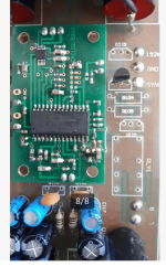
Power Supply for FIRST WATT amplifiers.
- By platon.rado
- Swap Meet
- 0 Replies
4x22.000uF 88.000uF per channel
2x 250W 2x19V
130€ + post EU
2x 250W 2x19V
130€ + post EU
Attachments
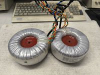
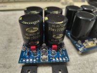
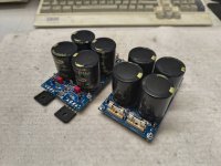
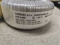
Hello there
- By Max12
- Introductions
- 1 Replies
Hey there, just joined the forum, currently planing on building myself some SyntripPs to go with my lonely TH12 tapped subwoofers
Greetings Maxi

Greetings Maxi
Help! AliExpress Crossover Values on Cerwin Vega E312
Hey, hoping for some observations on these crossovers I picked up for a little Cerwin Vega project I have planned with my brother. I have a set of Cerwin E-312 and the crossovers are really subpar.. So in thinking about stuff for the both of us to do as a project, I thought of redoing these speakers I have in my workshop.
Here is the crossover I picked:
https://www.aliexpress.com/item/1005005705670791.html
First off, I'd probably do some obvious things like remove the cheap screwed on terminals and solder wire direct. But in reading reviews, these Russian guys were all sounding off on incorrect values used on the LF portion - the 2.7uF specifically and how it should be larger. Having a look, trying to see what they are talking about, if anything at all. I'd also bypass a few caps too, maybe hard-wire the midrange jumper. Interested in some thoughts. Fortunately there was a pic posted of the backside of the PCB. What do you think of extras to do on these?
Transistor ONSEMI MJ21194 + Heatsinks
- By platon.rado
- Vendor's Bazaar
- 2 Replies
Transistors tested. Price 90€ + post. 16 pcs
Attachments
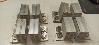
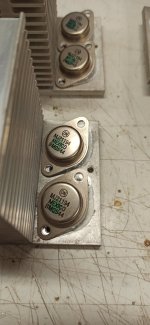
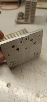
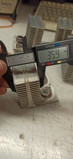
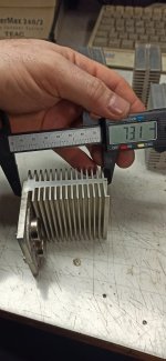
Sub phase alignment
- By stajo
- Subwoofers
- 16 Replies
Hi, I didnt know if I should ask here or at Multi Way but you dudes that are into subs might know. So I have done some repositioning of speakers and listening position etc and listening and measuring, trying to understand what happens. I have come up with a placement that suits me fairly for my LP and the speakers. It sounds ok, still doing tweaking with speaker stuffing (its TQWT) that changes things quite alot. Lately I have also added two subs that are placed ca 1,5 m in front of the speakers. I assumed that I will have to run those thru a dsp because of likely phase disalignment with the speakers woofers. But It doesnt sound or measure as I will have to.
The system is analog but actively crossed at 1000 hz, and I feed the subs with an extra buffer that I have tapped from the LF outputs on the active x-over, so they have a 20-1000 hz signal. The main speakers has a fairly good respons down to abt 40, than they fall pretty steep. So I turned the local low pass button on the subs all anticlockwise to lowest lowpass fq, hoping that they will cut over 40 or so. And maybe they do but not very steep, as seen in measures.
But, now to my main poll. Do you agree that it doesnt look like I have a big problem with phase woofer/subs, so maybe I can skip the dsp and work with some sub eq instead?
Lower is speakers only, both channels, upper is with subs added.
Old Theatre Projectors
- By walguzz 59
- Introductions
- 3 Replies
Hi, I am new to here, so i'm not sure how this all works yet, but getting there. I am seeing if anybody out there know's much about old movie projector's they used in theatre's years ago, when you had to make up the picture by splicing and threading the projector etc, and the reason being, that my Dad worked in this industry for most of his life. He is a Hoyt's Pioneer, and knew a lot about movie projector's, as well as his many friends he had in the industry. Sadly, now day's, he is in a nursing home with Dementia, and i have a few things like an old, but i think, functioning head off an old projector, and it appears very old, and a few funny looking Lens's, however, being technically challenged, i am not sure how to put pics on here, but could ask one of the Grand kid's i suppose, they are sure to know. There is also two old reals of movies, maybe 16mm or 8mm, not sure. Anybody else know much about these thing's? A couple of the Lens's are of a Schneider Brand, one is a Cine-xenon MC, Code 37 532. Anyway, if someone who is a bit knowledgeable about these thing's, i would like to hear from you. Thanks. Chris
modifying valve amp with net/single bias trimpot
- By lordearl
- Tubes / Valves
- 35 Replies
I've recently switched out a set of EL34 tubes in the attached circuit and find adjusting the bias a rather painful process as the adjustment is done on a net basis for both tubes and it is very hard to get the tubes matched to an acceptable level.
What would be the most efficient way to add in a second trimpot so each power tube could be adjusted separately?

What would be the most efficient way to add in a second trimpot so each power tube could be adjusted separately?
Semisouth goes Dodo ; what now ?
now , as wrenchone sez here , Semisouth goes Dodo .
SemiSouth closure to cost Calif. firm $60 million - San Jose Mercury News
if you're having any useful info about possible ( not left-kidney-right-leg price) SIC-SIT-JFET , put it here .
SemiSouth closure to cost Calif. firm $60 million - San Jose Mercury News
if you're having any useful info about possible ( not left-kidney-right-leg price) SIC-SIT-JFET , put it here .
Turntable with a synchronous motor
- By valleyvic
- Analogue Source
- 29 Replies
Hello all,
I want to ask your advise. It's about a turntable. I picked up one a few weeks ago. Cleaned it up, oiled, changed the belt, etc. Looks and works fine ... except for one thing.
I didn't notice that at once, only recently my ear raised a concern. Music sounded a bit faster on this player than on the other. Quick check by the RPM app revealed the reason - 35.5 rpm. No pitch control on this player, no strobe. It is a Sony PS-1350 with a 4-pole synchronous motor. Apparently it picks up its speed from the mains frequency. Mine as expected is solid 60 Hz. If that motor expects 50 Hz - that would explain the slight speed increase.
Any ideas how to correct/fix this?
Thanks.
Avalanche AS1 modernization
Avalanche AS1 was an active 3-way speaker made in early '90s in Finland by a small company in Eastern Finland.
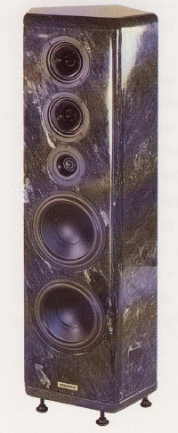
It is an active 3-way speaker with analog line level xo and three amplifier boards with Hitachi K135 MOSFET amplifiers.The box is made of soupstone, dead weight 86kg a piece! Drivers are ScanSpeak 21W/8555 (pair) Audax/Polydax 4" mids (pair) and a Dynaudio D28 tweeter.
This pair was for sale at a Finnish hifi-forum, and to my surprise I knew the owner! He had bought this pair just before the bankcrupcy of the company. The speakers had one bass drivers changed but still they suffered from poor sound.
I just had to push the buy button, but for totally altruistic reasons - I will give this pair to my younger son!
Simulating a swinging choke / saturating choke
- By 50AE
- Tubes / Valves
- 30 Replies
Hi folks,
I've been wondering, perhaps not in PSUD, but in LTSpice, is there a way to make a model of a saturating choke with the two following options:
1. Decreasing inductance vs DC current when used into a choke input filter, for the power supply of a class AB amplifier
2. Decreasing inductance vs AC voltage across the choke when used before the rectifier, same application.
EL34 PP output transformers
- By decramer
- Tubes / Valves
- 58 Replies
I have 2 output transformers from an ARTEC 225 amplifier (EL34 PP). The indication is 5000/30W and the EI-iron measures 92x78x64.
3 individual outputs (I call them A,B,C), a FB? (F) and a CT primary (D-E). I measured the impedance @ 1kHz:
An 8 ohm @ A gives 7 ohm @ B, 13.5 ohm @ C, 32k2 ohm @ D-E and 2k32 ohm @ F
An 8 @ B 4.2 ohm @ A, 12 ohm @ C, 24k5 ohm @ D-E 1k98 ohm @ F
An 8 @ C 2.65. @ A, 3.65 ohm @ B, 13k45 ohm @ D-E 1k24 ohm @ F
An 8 @ A-B in series , 7k64 ohm @ D-E 775ohm @ F
An 8. @ B-C , 4k79 ohm @ D-E 488 ohm @ F
An 8 @ A-C , 2k7 ohm @ D-E 280 ohm @ F
I would like to build an amp with ECC82 as phase shift and EF86 as input stage. I also have 2 power transformers each 100VA/ 700VCT 5V 6V3 an 2 GZ34's (=5AR4).
IK Multimedia IRIG PRO DUO No power
- By Paulmongan
- Analog Line Level
- 0 Replies
Hi folks,
I have an IK Multimedia IRIG PRO DUO which will not power up. I’ve tried it with the 2 AA batterys (3v line) and with a 9v bench power supply (9v input line) I opened it up and had a good look around. I don’t see any shorts or obvious comment damage. It’s pulling about 0.22mA when plugged into bench supply at 9v input no lights on . And it’s pulling 0 mA on the battery 3v supply. All fuses on the pcb are good. No obvious sign of component damage anywhere. I can trace the voltage past the fuses up to smd transistors but nothing then on the other side of transistors. Teo diodes back to back close to main fuse on 9v input are measuring 1.2v forward bias and open in reverse seems ok. . If I heat this area with iron I get power up to the blue lights. And looks like it is working. But dies away quickly when I remove the iron. I have tested the components on the power section and all seem good to me. It’s strange the 3v input has no current draw at all. If I was to post some pics of the pcb circuit and voltages would it be any help someone might under stand what is actually happening here.
Just wondering has anyone else had power issues with this unit and maybe had a fix.
This is a link to the unit I am trying to get working.
https://www.soundonsound.com/reviews/ik-multimedia-irig-pro-duo?amp
Thanks in advance
Ultrasound loudspeaker choose
Good morning gentlemen, I would like to purchase a loudspeaker for ultrasounds with a frequency greater than or equal to 20khz. But I'm here to ask you which loudspeaker to choose, piezoelectric transducers like those of ultrasonic cleaners or magnetorestrictive transducers like tweeters, I would like a lot of power 100W or more, and frequencies greater than 20khz. I hope you can help me, thanks
How to get help from a human at eBay?
- By Old bones
- The Lounge
- 11 Replies
I have wasted most of today trying to do just that. I am unable to log in due to some technical (?) glitch and that infuriating chatbot keeps shunting me down useless links to FAQs that don't even come close to addressing the problem. I managed to make contact with most of the employees of the ebay call centre in India but after listening to their well-rehearsed scripts of how wonderful I am for being an ebay member and they would be delighted to help, I am no closer to a solution. Does anyone know of a way to cut through the ******** to get help?
Cloning Energy Veritas 2.3
- By Websurfer81
- Multi-Way
- 0 Replies
Hi people.
I own a single speaker Energy Veritas 2.3 and drivers to make one more.
I don't have a second crossover neither a second cabinet.
I am planning to clone the crossovers and also the cabinets.
The question is..
The bass port system is not so easy to clone.
I can find almost the same dimensions on bass ports on the market but it would be placed flashed at the baffle without the edge outside of the cabinet.
Does this will change things dramatically?
I'm posting photos to give you an idea.
Thanks in advance.
Attachments
-
 IMG_20240627_155525.jpg139 KB · Views: 59
 -
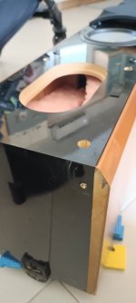 IMG_20240627_155426.jpg119.5 KB · Views: 54
 -
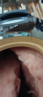 IMG_20240627_155403.jpg120.1 KB · Views: 48
 -
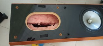 IMG_20240627_155355.jpg133.7 KB · Views: 48
 -
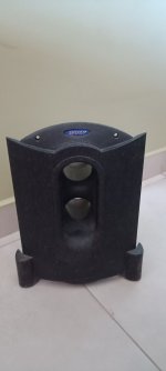 IMG_20240627_155336.jpg86.4 KB · Views: 47
 -
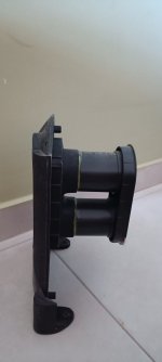 IMG_20240627_155324.jpg84.7 KB · Views: 58
 -
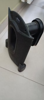 IMG_20240627_155303.jpg101.3 KB · Views: 51
 -
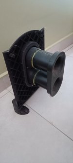 IMG_20240627_155250.jpg91.1 KB · Views: 49
 -
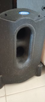 IMG_20240703_171230.jpg185.5 KB · Views: 51
 -
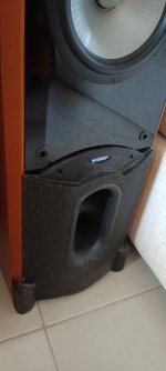 IMG_20240703_171151.jpg135.9 KB · Views: 51
 -
 IMG_20240703_171101.jpg105.9 KB · Views: 55
Construction of acoustic box with several woofers
- By Radew
- Construction Tips
- 25 Replies
Hi everyone,
I am starting a project to design an audio system for my home by reusing different woofers that I have taken from different speakers, systems, etc.
I read a student's thesis from 2009 on sound engineering and acoustics, and on the calculation and design of an acoustic box for a JBL woofer.This paper helped me a lot to understand the calculations behind the design of acoustic boxes, and to be able to calculate a box for my woofers.
The problem is that the design exemplified in the thesis is about a box for a single woofer, and I have several woofers, with different Thiele-Small parameters, which come from very different audio fields, so I don't know how to calculate a box. to be able to have all the woofers in the same box, or if it is not possible. I also don't know how I can see the theoretical response of the box with the woofers, since in programs for this, like WinSID (which is the one I use) you can only see the behavior of one or more woofers, but of the same model, not of different models.
So my main doubts are, how can I calculate the same box for the same woofers, given that they are different models, and with different Thiele-Small parameters. And my other question is also how can I see the theoretical response of the box?
I would also like to be able to better understand the Bode plot implemented for the responses of the woofers, since I do not understand it 100%
Any kind of advice, tips, etc. I would also greatly appreciate it.
PD:I don't speak English that well, so all this writing was translated by Google Translate, in case there are strange things in the writing, hahaha
Denon PMA355UK Selector Switch Replacement
- Solid State
- 4 Replies
Hi I have one of the above amplifiers and it randomly jumps the input. I believe this is due to a worn/dirty rotary selector control. So I thought I'd source a replacement part, but have been unable to find one online. I did find one for the PMA535R on ebay, which looks the same (https://www.ebay.co.uk/itm/154325062392) so does anyone know if the PMA535R one would work with my PMA355UK. Also asuming it doesn't would acquiring a remote control and using that to change input channels provide an alternative. If not can anyone recommend a good repair technician in the UK, preferably Bournemouth and surrounds that might be able to clean and fix the switch?
Class-D Guitar full range amp for modellers (TPA3255 based) recommendations (speakers, etc)
- By Harehare
- Instruments and Amps
- 24 Replies
Hi,
I am planning a class D guitar amp:
Ideally it should be full range - so it can be used for other instruments ... if needed. I need advice ... especially for speakers. Coaxial would be preferred, but with max price around 100 USD per piece. Other ideas are also welcome.
I someone has made similar build ... I would be happy if he/she could chime in.
cheers
I am planning a class D guitar amp:
- TPA3255 based amp
- stereo 2 x 120w into 8 ohm
- either 6.5" or 8" speakers
- coaxial or extended range
- compact enclosure
Ideally it should be full range - so it can be used for other instruments ... if needed. I need advice ... especially for speakers. Coaxial would be preferred, but with max price around 100 USD per piece. Other ideas are also welcome.
I someone has made similar build ... I would be happy if he/she could chime in.
cheers
Darling 1626 Amp
- By jcmusic
- Tubes / Valves
- 18 Replies
I picked up this little amp a few weeks ago and was just wondering if anyone here could offer advice on tubes to improve or change the sound?
Here are the details from the builder in 2010.
I built this little amp about 6 months ago and it's seen about 25 hours of use. You could think of the amp as a JE Labs "Simple 45" except it uses the 1626 output tube (the schematics are virtually identical except for output tubes and naturally different operating points).
The tubes include a 5U4GB rectifier, a pair of 1940's Hytron 1626 power tubes and an RCA JAN Black Plate (graphite coated envelope) 12SL7 driver tube (all tubes were new with the amp and have about 25 hours on them max).
I've really enjoyed this amp in my Den and used it to drive some custom made 94 DB single driver speakers with plenty of volume and dynamics for my listening level. The tube puts out about .75 watts per channel so more efficient speakers will be needed in a larger room. However, I let one of my friends with a pair of Lowther Alerion speakers at around 94 db efficiency listen to it in his larger room and he really liked it. But he already has two of my hand built amps and couldn't really justify buying another one (he has several other tube amps as well) so this one is available to the public at large.
The amp has an overbuilt power supply and is really quiet. I used a seperate filament transformer with center tap to help with hum balance and avoid any coupling noises between windings in the power transformer which I think helped.
Some other details about the amp:
-- NOS USA Made Pyramid Paper in Oil Coupling Capacitors
-- Teflon Jacketed Silver Clad copper for all signal carrying wires.
-- Made in USA new Edcor output transformers
-- Super short signal path, with an attempt to use only the leads on most resistors to minimize the number of solder joints.
-- Lead free Kester 3% silver solder used exclusively
-- Vintage Power transformer that I picked up on Ebay last Summer (spray painted it a hammertone black to match the plinth).
-- A hybrid star ground that uses a short silver clad copper bus bar that is reputed to be quieter than a straight star ground (high currents are kept from commingling with sensative signal circuits).
The amp is point to point wired, although I did build the power supply on a perf-board to conserve space and to better group the power supply grounding node.
Beyma TPL150 TPL200 or Mundorf AMT28 AMT29?
Hi to everyone.
What is better about sound from these Heil?
I see on datasheets, Beyma little bit better.
What is better about sound from these Heil?
I see on datasheets, Beyma little bit better.
Load more
Projects by fanatics, for fanatics
Get answers and advice for everyone wanting to learn the art of audio.
Join the Community
507,774
Members
7,888,010
Messages