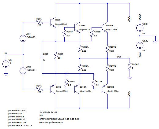
I picked the bias voltages VB1 and VB2 to get bias currents of 150 mA in each device with an open-circuit load. This was the current that Bob Cordell used in his original MOSFET error correction amp AES article. Since there's no optimum bias for FETs as there is for bipolars, the choice is somewhat arbitrary - the more, the better as far as distortion.
For the two offset voltages V3 and V9, I picked these so that V(out) = 0 when V(in) = 0. I guess this is somewhat arbitrary, and maybe unnecessary. I did this by first setting these voltages to zero, then finding the output DC voltage of each circuit with an open-circuit load. Then I set each one to the negative of its corresponding output offset, and reconnect the load. This usually gives an output offset within microvolts of zero with the load connected.
For the two offset voltages V3 and V9, I picked these so that V(out) = 0 when V(in) = 0. I guess this is somewhat arbitrary, and maybe unnecessary. I did this by first setting these voltages to zero, then finding the output DC voltage of each circuit with an open-circuit load. Then I set each one to the negative of its corresponding output offset, and reconnect the load. This usually gives an output offset within microvolts of zero with the load connected.
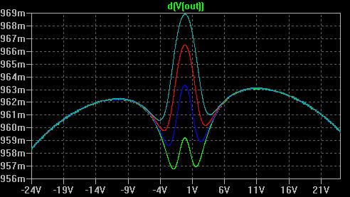
one thing i have found useful in LTSPICE is to plot the input waveform minus a portion of the output waveform (like this: V(in)-(V(out)/20) the number 20 represents the amp gain, and can be whatever number the gain is). this gives a waveform of the distortion residual. this will also show you if you have crossover distortion, since the spikes will be clearly visible. your residual may also seem to be out of phase, and i.m not really sure yet how to compensate for that.
the way to plot this is to wait for the simulation to finish, click on plot, select Add Plot, and insert the formula in the numeric expression box.
the way to plot this is to wait for the simulation to finish, click on plot, select Add Plot, and insert the formula in the numeric expression box.
Nice job, Andy. How many hours I've spent on that !
gives
I guess that setting the offset (that is needed if one merely plots V(out)/V(in) since when V(in)=0 also V(out) need to be zero, otherwise you have a singularity) is unessential because you are dealing with d(V(out)).
Thanks again
gives
I guess that setting the offset (that is needed if one merely plots V(out)/V(in) since when V(in)=0 also V(out) need to be zero, otherwise you have a singularity) is unessential because you are dealing with d(V(out)).
Thanks again
I have the 2SJ201 EKV subcircuit model parameters extracted now.
First, I wanted to mention about the optional series drain resistor. This applies to both the 2SK1530 we've talked about and to the 2SJ201. The EKV model seems to greatly underestimate the ON resistance of the devices, simulating them at about 0.05 Ohm with Vgs = 5V. For the 2SK1530 LTSpice model I previously posted, there is a series drain resistance of 0.383 Ohms to bring this to the correct value. I have some worries that this might cause some undesired side effects, so if you're concerned about this, just replace it with a 1m resistor in the subcircuit. Same for the 2SJ201 model.
I've attached a zip file with the 2SJ201 information. This includes the Excel spreadsheet used to extract the parameters, an LTSpice symbol file, the subcircuit text file, and a couple of simple test circuits.
I got the Cgs value in a slightly different way than for the 2SK1530. For that device, I just computed Ciss - Crss at one Vds value. For the 2SJ201, I subtracted the entire curves and took the average of the difference. This should average out some of the pixellation in the captured capacitance graph data.
You'll also notice that the spreadsheet treats the devices as "pseudo N-channel" devices, where the drain current and Vgs measured data must be entered as positive numbers. There is a boolean variable "IsNChan" that tells the code which type of device it is. Once the parameters of the EKV model are extracted, the only change that's necessary is to change the sign of the threshold voltage. This approach simplifies things and helps prevent errors in the VBA code for the EKV function.
Attachments
I had a slight problem with Cgd in the subcircuit file starting out. At first, I just replaced "<" with ">" in the "if" statement, but that is an error. The argument to "atan" must always be negative, and for "tanh" must be positive. So I just swapped the G and D nodes in the nonlinear capacitance connection and kept the "if" expression the same. This had me scratching my head for a while, with completely wrong simulated capacitance values ") .
.
.EKV models
Hi Andy,
As you already said, fitting my measured data for Id vs. Vgs together with the data sheet values is kind of a tricky business (private communications). Nevertheless, everything went fine with the 2SK1530. It's the p-channel that's hard to fit.
Having looked at the 2SJ201 data more carefully, it's becoming clear to me that we will never succeed to join both data sets together. The 2SJ201 according to the data sheet differs too much from the few samples I have once bought.
What to do now? If we use the model based on the data sheet, we have a serious problem, as the distortion in a typical output stage is too high. I know this, as I have spiced Bob Cordell's EC amp. This model gives a THD20 of 9ppm (BW=150kHz), while the model based on my measurements results in THD20 = 6ppm, exactly the same as the real distortion.
I heavily suspect the Id-Vgs curves on the data sheet. Maybe you should use the curves of the forward admittance in stead, as these cover a larger range of drain currents and can be digitized with more accuracy. However, these data will not solve all discrepancies, as the values are about 30% lower than mine.
Cheers, Edmond.
Re: EKV models
Hey guys, I really appreciate your work here. I can't wait to simulate a MOSFET output stage for distortion with some confidence, with or without EC. If I can be of any help, please let me know. I think I have some of these MOSFETs, and I could take some real measurements if that would help.
Cheers,
Bob
Edmond Stuart said:Hi Andy,
As you already said, fitting my measured data for Id vs. Vgs together with the data sheet values is kind of a tricky business (private communications). Nevertheless, everything went fine with the 2SK1530. It's the p-channel that's hard to fit.
Having looked at the 2SJ201 data more carefully, it's becoming clear to me that we will never succeed to join both data sets together. The 2SJ201 according to the data sheet differs too much from the few samples I have once bought.
What to do now? If we use the model based on the data sheet, we have a serious problem, as the distortion in a typical output stage is too high. I know this, as I have spiced Bob Cordell's EC amp. This model gives a THD20 of 9ppm (BW=150kHz), while the model based on my measurements results in THD20 = 6ppm, exactly the same as the real distortion.
I heavily suspect the Id-Vgs curves on the data sheet. Maybe you should use the curves of the forward admittance in stead, as these cover a larger range of drain currents and can be digitized with more accuracy. However, these data will not solve all discrepancies, as the values are about 30% lower than mine.
Cheers, Edmond.
Hey guys, I really appreciate your work here. I can't wait to simulate a MOSFET output stage for distortion with some confidence, with or without EC. If I can be of any help, please let me know. I think I have some of these MOSFETs, and I could take some real measurements if that would help.
Cheers,
Bob
My position is that I've already spent much more time on this project than I had anticipated. It's getting in the way of a project I'm working on. I'm not even using these Toshiba devices myself anyway.
I've provided the spreadsheet that fits the parameters. Everything needed to fit the parameters is there. Edmond has measured data for the devices that goes up to 3A. That data could be entered into the appropriate cells of the spreadsheet and new parameters computed. I'm willing to explain that process, but I'm not going to allow myself to be caught up in an infinite time sink.
I've provided the spreadsheet that fits the parameters. Everything needed to fit the parameters is there. Edmond has measured data for the devices that goes up to 3A. That data could be entered into the appropriate cells of the spreadsheet and new parameters computed. I'm willing to explain that process, but I'm not going to allow myself to be caught up in an infinite time sink.
EKV models
And here is the EKV model of the p-channel device, adapted to Micro-Cap (MC8 and MC9).
Notice that this model, opposed to Andy's one, does not represent the average characteristics of the 2SJ201, rather the particular properties of just one sample. Nevertheless, it works really nice in conjunction with the n-channel model shown here:
http://www.diyaudio.com/forums/showthread.php?postid=1317949#post1317949
Once again Andy, thank you very much for all the good work you have done for the Spice community.
.SUBCKT 2SJ201EKV 1 2 3
* Node 1 -> Drain
* Node 2 -> Gate
* Node 3 -> Source
***************************
+PARAMS: Cgdmin = 143p
+PARAMS: Cgdmax = 2677p
+PARAMS: a = 0.31548599
+PARAMS: B = { ( Cgdmin + 0.5 * pi * Cgdmax ) / ( 1 + 0.5 * pi ) }
+PARAMS: C = { ( Cgdmax - Cgdmin) / ( 1 + 0.5 * pi ) }
M1 4 5 3 3 PMOS44
RG 2 5 1m
RD 1 4 1m
;RD 1 4 0.198
DDS 1 3 DDS
CGS 5 3 1414p
GGD 2 1 VALUE={ if( V(2,1) < 0, -C * tanh( a * V(2,1) ) + B, -C * atan( a * V(2,1) ) + B ) * DDT(V(2,1)) }
.MODEL PMOS44 PMOS ( LEVEL=44 L=2U W=0.5m
;+ EKVINT = 1
+ cox = 3.6e-4
+ xj = 2e-7
+ vto= -1.72 ; threshold voltage, adjust this value at will
+ gamma=6
+ phi=2.4
+ kp=8.5e-2
+ e0=2.0e+11
+ ucrit=2.67e+13
+ dl=0 dw=0
+ lambda=1.1305e5
+ ibn=1.0 iba=0 ibb=3.0e8
+ weta=0.0 q0=0 LK=2.9e-7
+ leta=0.0 rsh=0.0 )
**********************************************************************
.MODEL DDS D( N=1.55178 IS=2e-8 RS=0.01 CJO=1544p M=0.4786242 VJ=0.423139 BV=200 )
**********************************************************************
.ENDS
Cheers, Edmond.
unclejed613 said:one thing i have found useful in LTSPICE is to plot the input waveform minus a portion of the output waveform (like this: V(in)-(V(out)/20) the number 20 represents the amp gain, and can be whatever number the gain is). this gives a waveform of the distortion residual. this will also show you if you have crossover distortion, since the spikes will be clearly visible. your residual may also seem to be out of phase, and i.m not really sure yet how to compensate for that.
the way to plot this is to wait for the simulation to finish, click on plot, select Add Plot, and insert the formula in the numeric expression box.
Sorry if it seems dumb, but does this mean if I perform this expression with say a .tran command, and I get a good squarewave thousand times less then V(out), the sim'd distortion is 0.001 without too many nastienesses?
Rüdiger
if your gain is .001 compared to V(in), then the expression will still result in a nasty trace. i've tried running the .FOUR command on numeric expressions, rather than actual voltage nodes, and it doesn't work. in any case, your distortion is weighted to the fundamental in the measured waveform, so whether you use .FOUR, or use FFT, you will still come out with huge distortion figures for a square wave. using V(in)-(V(out)/Av) will only give you a waveform with most of the fundamental cancelled out, leaving the distortion residual, and this will usually be a very nasty looking waveform, containing any crossover notch, clipping products, noise, and anything else that wasn't included in the input waveform.Onvinyl said:
Sorry if it seems dumb, but does this mean if I perform this expression with say a .tran command, and I get a good squarewave thousand times less then V(out), the sim'd distortion is 0.001 without too many nastienesses?
Rüdiger
I cannot agree on that. With a reasonably small time step (preferably using a prime number ratio) I found the harmonics (via .FOUR) of the sine generator to be 180dB down (which seems to be a PC implementation limit -- I have yet to find a software generator with lower distortion than that). Of course with compression off (.opt plotwinsize=0), and using the alternate, higher precision solver.unclejed613 said:i've tried running the .FOUR command on numeric expressions, rather than actual voltage nodes, and it doesn't work.
FWIW, this might be of interest for the distortion simmers, dealing with BJT EF output stages:
http://www.diyaudio.com/forums/showthread.php?postid=1299540#post1299540
- Klaus
teodorom said:Nice job, Andy. How many hours I've spent on that !
gives
I guess that setting the offset (that is needed if one merely plots V(out)/V(in) since when V(in)=0 also V(out) need to be zero, otherwise you have a singularity) is unessential because you are dealing with d(V(out)).
Thanks again
Very nice display. Can you post the LTSpice asc file you used for this?
Thanks,
Bob
what i meant was, i think i tried something like .FOUR 1KHZ (V(IN)-(V(OUT)/20)) and it didn't work, but .FOUR 1KHZ V(OUT) or .FOUR 1KHZ V(N003) will work.
or maybe it was the .WAVE command that didn't work. i can't think of a reason to use a .FOUR command on a numeric expression, but since the .WAVE command requires input of less than +/- 1V, then it would be convenient to use .WAVE test.wav 44100 (V(OUT)/20) for an amplifier output, but i tried it, and got no output to the file.
or maybe it was the .WAVE command that didn't work. i can't think of a reason to use a .FOUR command on a numeric expression, but since the .WAVE command requires input of less than +/- 1V, then it would be convenient to use .WAVE test.wav 44100 (V(OUT)/20) for an amplifier output, but i tried it, and got no output to the file.
Ah, ok. I tried that, seems like the expression parser quite simple. It uses the first node found within a complex expression, unless the expression starts with something else than a node. So (V(IN)-(V(OUT)/20)) will give just V(IN), but something like (-0.05*V(OUT)+V(IN)) will produce an error msg.unclejed613 said:what i meant was, i think i tried something like .FOUR 1KHZ (V(IN)-(V(OUT)/20)) and it didn't work, but .FOUR 1KHZ V(OUT) or .FOUR 1KHZ V(N003) will work.
Similar behaviour here. Either only first node taken, or error.or maybe it was the .WAVE command that didn't work. i can't think of a reason to use a .FOUR command on a numeric expression, but since the .WAVE command requires input of less than +/- 1V, then it would be convenient to use .WAVE test.wav 44100 (V(OUT)/20) for an amplifier output, but i tried it, and got no output to the file.
If just the node name alone is given, without V(..) or I(..), then the voltage is taken, I found out BTW
One can avoid that with a simple BV device generating a voltage from an arbitrary expression.
- Klaus
- Home
- Design & Build
- Software Tools
- Spice simulation