Would you be interested in testing the switching power modules?
Not until I've tested a real prototype...
")
After that it could be interesting.
It may be worth looking at this to get an idea where return currents flow, dc follow path of leat resistance as the frequency get higher the return currents will flow (or want to flow) under the signal trace, path of least inductance, especialy important for rf frequecies (ie noise) but also for audio frequencys as they span the area where the return current path is moving from resistance to inductance.
I've read that document, together with a lot more... an instructive reading.
In fact I've tried to follow all of the suggested best practices but since I'm not an expert every suggestion is welcome.
I interpret that as the problem for those not versed in Ground Plane Design.
Unintended parasitics !!
In this particular case the added capacitance on PS traces shouldn't be a problem, actually it should be welcome...
In the signal area, to the contrary, it could be a problem, particularly near the opamp and on the current pump, it's for this reason that I've reduced the top plane.
But I could be wrong, I'm not an expert, any opinion and/or suggestion is, as always welcome.
In fact in the Evolution PCB there are multiple top ground planes over the opamp and the current pump too... but traces are narrower.
Having a ground plane become a necessity above 1MHz, for return current coupling, and having a GND plane is critical to reducing trace inductance,
this is important for noise, especially any coupled high frequency noice and RF.
and having a ground plane for analogue is common practice (well in mil.areo and medical analogue), as I have stated befor,
when I started doing PCB design in the mid 80's ALL analogue designs had ground planes, whereas some digital designs would
be two layer designs with a gridded power and return traces.
I often hear comments that indicate people dont understand ground planes, yet will mess about with return current traces,
whereas having a GND plane will allow these currents to find their own path, dependant upon frequency, home; would reduce magnetic coupling (noise)
and lower the inductance of the PCB traces. Trace resistance is often discussed, but with any AC trace impedance is as important and of all the
parasitics inductance is probably the most important, especialy with the amount of RF noise generated (mobile phones, WiFi etc etc).
The capacitance I quoted was for a wide power track, when you get down to signal traces over a ground plane the figures are samll, for a 0.2mm (8 thou)
trace, 1oz copper double sided PCB FR4 dielectric (approx Er 4.2) its about 0.037pf/mm, so is pretty small (Zo = 147 ohms). To get a 75 ohm Zo you require
a 1.5mm wide trace for a double sided PCB, this drops to 0.25 (10 thou) for a standard 4 layer PCB (note if you wanna match any impedences of traces
etc such as SPDIF). This also illustrates the importance of a ground plane for lowering inductance.
I would reccomend to anyone who is serious about design today to try and get hold of a copy of Henry Ott's Electromagnetic Compatability Engineering.
http://www.speedingedge.com/PDF-Files/BTS006_What_Is_Inductance (2).pdf
http://www.polarinstruments.com/support/cits/IPC1999.pdf
Some Standard Multilayer PCB builds for Info:
http://www.merlincircuit.co.uk/Downloads/4layer.pdf
http://www.merlincircuit.co.uk/Downloads/6layer.pdf
Having a ground plane become a necessity above 1MHz, for return current coupling, and having a GND plane is critical to reducing trace inductance,
this is important for noise, especially any coupled high frequency noice and RF.
and having a ground plane for analogue is common practice (well in mil.areo and medical analogue)
Hi Marce,
I've read all your links, some were known, others not... a very interesting reading
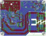
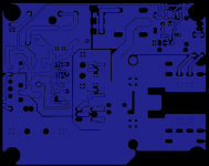
Basically the PCB is my effort to apply such suggestions but, since this is the first PCB that I design, I've a lot of doubts...
I've also took inspiration from various real world PCBs of audio gear from my service manuals collection...
I would appreciate very much if you can point me to something you consider critical on the PCB or suggest one or two improvements, in fact I've started the thread for this reason...
Some PCBs even have heat sink cores in the layers. High power RF layout probably is more critical, and if such can be studied, might shed more light on the issues involved. For a simple circuit like this, it probably is already as good as it could get. Generally we don't want returns too much in parallel with it's signal trace if the currents and voltage variation is above a certain levels, unless they might exactly cancel out. I have experimented somewhat with speaker cables, and expect to take it further in time.
Marce,
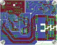
maybe the attached design is a step forward?
Dear ClaveFremen,
I like the fact you consider a ground plane design. Thanks to the help of Marce on this forum and Henry Ott I succeed successfully in commercial designs to incorporate ground plane design for multichanel high and low current circuits all on the same board without any humm or noise whatsoever. My subjective opinion is that audio designs with good designed ground planes sound much better.
If you want to do it really good, I advice you to raise the cost a bit and go for a 4 layer PCB. Make layer 2 a unbroken ground plane.
The problem with 2 layer designs and ground planes is, That the plane is broken on many places. The return current above certain frequencies want to follow the path of least inductance. Broken ground planes can block those routes.
If you see the circuit as a shower and a drain and visualize it that way, you can actually control big and small currents better then one might think. It is all about discipline of circuit and component placing. Close all current loops individually and make sure the low current circuits aren't in the loop of the high current circuits. Shower and drain....
Good luck!
With kind regards,
Bas
Dear ClaveFremen,
Another note. Keep differential pairs always tightly coupled with coupled parallel traces. This is for the +/- 15VDC supplies for the opamp, but also for the main PSU lines. In your design the two traces are not consistently parallel. Keep them together close and treat them as a parallel pair.
With kind regards,
Bas
Last edited:
Generally we don't want returns too much in parallel with it's signal trace if the currents and voltage variation is above a certain levels, unless they might exactly cancel out.
I've attached the Eagle files, so, if you want, you can have a more 'inside' look...
I like the fact you consider a ground plane design. ...
My subjective opinion is that audio designs with good designed ground planes sound much better.
Hi Bas,
your experience with ground planes is encouraging. Thanks
If you see the circuit as a shower and a drain and visualize it that way, you can actually control big and small currents better then one might think. It is all about discipline of circuit and component placing. Close all current loops individually and make sure the low current circuits aren't in the loop of the high current circuits. Shower and drain....
Another note. Keep differential pairs always tightly coupled with coupled parallel traces. This is for the +/- 15VDC supplies for the opamp, but also for the main PSU lines. In your design the two traces are not consistently parallel. Keep them together close and treat them as a parallel pair.
I've made a new revision trying to follow your suggestions, you'll find it attached.
Any opinion is welcome.
If you want to do it really good, I advice you to raise the cost a bit and go for a 4 layer PCB. Make layer 2 a unbroken ground plane.
The problem with 2 layer designs and ground planes is, That the plane is broken on many places. The return current above certain frequencies want to follow the path of least inductance. Broken ground planes can block those routes.
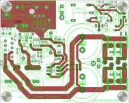
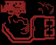
See the attached top and bottom PCB traces, to me the top 0V and GND planes seems good.
The bottom 0V and the GND planes are there just to better isolate traces and reduce crosstalk, at least this is my goal...
Attachments
Dear ClaveFremen,
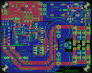
I like what you did with the power amp PSU traces. And it is indeed a very good thing that the ground-plane underneath those traces isn't broken.
It would be nice if you can do the same for the opamp PSU traces, which are not yet totally a parallel pair.
Personally I am not really fond of having two ground-planes overlapping on different layers. I would stick with just one ground-plane only on the bottom layer.
I think you nailed the design down in many ways and you did a very good job. However if one would nitpick, it would be even nicer if the opamp wasn't buried between on the left the LM3886 and on the right the PSU rails. (It is kinda in the "U" shape). The magnetic fields from both sides will radiate through the low current line stage.
If possible and you want to go that far, Try to keep all the high current on one side, and place the op-amp together with the rest of the line signal traces on the other side.
Also, why is there a cut between the PGND connection and the rest of the ground-plane? Can you remove that one?
With kind regards,
Bas
Last edited:
I like what you did with the power amp PSU traces. And it is indeed a very good thing that the ground-plane underneath those traces isn't broken.
Hello Bas,
thanks
It would be nice if you can do the same for the opamp PSU traces, which are not yet totally a parallel pair.
I've tried but I can't figure out how with those TO220 LM3x7, or with transistors and caps is a so tight space.
The test circuit (on breadboard) is using TO92 LM3x7 but they get too hot, 66°C, aren't they?
Personally I am not really fond of having two ground-planes overlapping on different layers. I would stick with just one ground-plane only on the bottom layer.
I'll check but I like the idea of having some copper to shield that delicate area.
I think you nailed the design down in many ways and you did a very good job. However if one would nitpick, it would be even nicer if the opamp wasn't buried between on the left the LM3886 and on the right the PSU rails. (It is kinda in the "U" shape). The magnetic fields from both sides will radiate through the low current line stage.
If possible and you want to go that far, Try to keep all the high current on one side, and place the op-amp together with the rest of the line signal traces on the other side.
Sadly, in 100x80mm (the maximum size allowed by the free edition of Eagle) I don't have alternatives...
The shielding plane is there in hope to mitigate this problem
Also, why is there a cut between the PGND connection and the rest of the ground-plane? Can you remove that one?
I've retained that last slot thinking about your shower and drain...
The idea is to avoid that return currents from the power traces passes through the lower voltage LM318 PS.
I know that in that way they probably radiate but I really don't know what is better...
Thanks Bas, this is the kind of help I'v was hoping for.
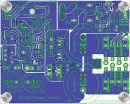
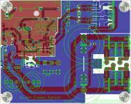
Dario, great work so far. The one thing on the original layout
which can be improved is the placement of the Out terminal.
Here's a quick-n-dirty stab to give an idea what I mean.
The txt file is the Eagle brd file renamed to make the forum s.w happy.
which can be improved is the placement of the Out terminal.
Here's a quick-n-dirty stab to give an idea what I mean.
The txt file is the Eagle brd file renamed to make the forum s.w happy.
Attachments
Dario, great work so far. The one thing on the original layout
which can be improved is the placement of the Out terminal.
Here's a quick-n-dirty stab to give an idea what I mean.
The txt file is the Eagle brd file renamed to make the forum s.w happy.
I think the OUT and return should be located further away from the small signal components. The last thing you want is the electromagnetic field coupling induced signals back though the gain stages to be amplified again.
Dario, great work so far. The one thing on the original layout which can be improved is the placement of the Out terminal.
Thanks
You're right but I can't agree with your solution, look:
I think the OUT and return should be located further away from the small signal components. The last thing you want is the electromagnetic field coupling induced signals back though the gain stages to be amplified again.
Soongsc is right, IMHO, instead, maybe, we could move the OUT GND near OUT... reversing the position of the DC protection circuit... I'll check.
Dear ClaveFremen,
...
I think you nailed the design down in many ways and you did a very good job. However if one would nitpick, it would be even nicer if the opamp wasn't buried between on the left the LM3886 and on the right the PSU rails. (It is kinda in the "U" shape). The magnetic fields from both sides will radiate through the low current line stage.
If possible and you want to go that far, Try to keep all the high current on one side, and place the op-amp together with the rest of the line signal traces on the other side.
...
With kind regards,
Bas
I second this comment. There was one design that did not separate these in another amp, and the sound was messed up compared to the prototype. I had to use the THD measurement (not that I normally use it) to convince them they messed up so my case was supported. When they fixed the layout, the sound quality and THD measurements compared well against the prototype.
Great point.
Thanks
You're right but I can't agree with your solution, look:
Soongsc is right, IMHO, instead, maybe, we could move the OUT GND near OUT... reversing the position of the DC protection circuit... I'll check.
Sure, whatever is best.
Can any ideas from the X-Calibre be applied ?
http://www.diyaudio.com/forums/chip...-hot-rodding-mauro-penasas-lm3886-design.html
http://www.diyaudio.com/forums/chip...-hot-rodding-mauro-penasas-lm3886-design.html
or move the entire power supply to another PCB ? Then you would have plenty of room to try 4 caps, MUR 10100, TeddyReg or even supply for LM318 or LF01What if we dump the DC protection to an external PCB?
Room to grow, room to play ?
What ever you decide, if there is a group buy I want some please sir.
Last edited:
or move the entire power supply to another PCB ?
I've already answered to this question on the previous thread.
Penasa was also skeptic about the separate PS.
Then you would have plenty of room to try 4 caps, MUR 10100, TeddyReg or even supply for LM318 or LF01
Room to grow, room to play ?
The actual PS is quite good, if only I could squeeze the space for two more caps (like in the 'eretic')...
What ever you decide, if there is a group buy I want some please sir.
No problem, at the end a PCB + smd parts GB is possible.
- Status
- This old topic is closed. If you want to reopen this topic, contact a moderator using the "Report Post" button.
- Home
- Amplifiers
- Chip Amps
- My_Ref Fremen Edition - need help on PCB evaluation