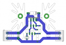
Here's what I mean.
- Due to the heatsink and the mounting holes you have a lot of space. Use it. Don't make the traces as thin as necessary, make them as thick as possible without sacrificing clearance.
- I don't like dual layer boards. They're more expensive to make and a PITA if you have to desolder lots of parts. Think from a service-standpoint. If you have to desolder a part for three or four times, what kind of pad will last longest? A small, plated-through one or a big one? If space permits, beef up the pads (I didn't, in this case). Those Eagle parts are nice for densely packed boards, but if you have some space left, go for it.
- The grid is there to make life easier. Don't use such a small grid! Start out with 25mil as a standard and go for 5mil if you need something more delicate. Use mm only for dimensions and mounting holes if that actually matters.
- See that little arrow at the heatsink? That's where the part is supposed to be placed. It will work with 25mil grid, try it") .
.
- Ground planes are not necessary for an old linear regulator. While they leave you with a lot of copper, they may make things worse due to cluttering up all your boardspace. That may not be a problem if the board is of good quality and uses a stop mask, but I prefer some nice tracks in this case.
- Think of vias as prone to failure, especially if there's only one of them right in the middle of the track which runs the highest current of the board! Avoid them as much as possible! Lazy people use vias. And autorouters, of course. If you have to, use some more of them to get a better current stability for those tracks running high currents.
- Mirror SMD parts and they will be placed on the bottom layer.
- You may place R1 vertical, as this would save a lot of space. Makes for shorter traces, but hey, we have the space.
- If running Input to Output from left to right is a must for you, try rotating the LM317 by 180 degrees, so that routing gets easier for you. If that doesn't lead to any difficulties with mounting (and I doubt that), do it - the part doesn't care about the orientation.
- The 1N4148 might be a little weak for this purpose. Since it's a fail-safe part, it should be able to withstand some current. Use something like a 1N400x, maybe even two of them in parallel. The space is all there.
Hopefully I didn't scare you...
- Due to the heatsink and the mounting holes you have a lot of space. Use it. Don't make the traces as thin as necessary, make them as thick as possible without sacrificing clearance.
- I don't like dual layer boards. They're more expensive to make and a PITA if you have to desolder lots of parts. Think from a service-standpoint. If you have to desolder a part for three or four times, what kind of pad will last longest? A small, plated-through one or a big one? If space permits, beef up the pads (I didn't, in this case). Those Eagle parts are nice for densely packed boards, but if you have some space left, go for it.
- The grid is there to make life easier. Don't use such a small grid! Start out with 25mil as a standard and go for 5mil if you need something more delicate. Use mm only for dimensions and mounting holes if that actually matters.
- See that little arrow at the heatsink? That's where the part is supposed to be placed. It will work with 25mil grid, try it
.- Ground planes are not necessary for an old linear regulator. While they leave you with a lot of copper, they may make things worse due to cluttering up all your boardspace. That may not be a problem if the board is of good quality and uses a stop mask, but I prefer some nice tracks in this case.
- Think of vias as prone to failure, especially if there's only one of them right in the middle of the track which runs the highest current of the board! Avoid them as much as possible! Lazy people use vias. And autorouters, of course. If you have to, use some more of them to get a better current stability for those tracks running high currents.
- Mirror SMD parts and they will be placed on the bottom layer.
- You may place R1 vertical, as this would save a lot of space. Makes for shorter traces, but hey, we have the space.
- If running Input to Output from left to right is a must for you, try rotating the LM317 by 180 degrees, so that routing gets easier for you. If that doesn't lead to any difficulties with mounting (and I doubt that), do it - the part doesn't care about the orientation.
- The 1N4148 might be a little weak for this purpose. Since it's a fail-safe part, it should be able to withstand some current. Use something like a 1N400x, maybe even two of them in parallel. The space is all there
.Hopefully I didn't scare you...
Attachments
Thanks Lasse. After your message last night I was thinking that having the heat sink on the other side of the board would help. I'm new to this so not at all afraid of receiving helpful comments! Thanks yet again!
Ps. In my revision I did beef up the pads for the resistors to make them easier to solder. I'm getting a little more confident editing devices/packages.
Ps. In my revision I did beef up the pads for the resistors to make them easier to solder. I'm getting a little more confident editing devices/packages.
Last edited:
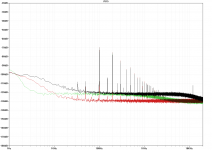
This time I tested the ubiquitous 7815 for comparison.
Noise-wise it actually performs quite well, a simple 317 without C-adj is a lot worse, but have a look at the difference in step response!
The black trace is for the 7815, green shows #400 (Zener) and red #302EX (with the low-noise Sipex 431) for comparison.
Noise-wise it actually performs quite well, a simple 317 without C-adj is a lot worse, but have a look at the difference in step response
!The black trace is for the 7815, green shows #400 (Zener) and red #302EX (with the low-noise Sipex 431) for comparison.
Attachments

Here's what I mean.
- Due to the heatsink and the mounting holes you have a lot of space. Use it.
Hi. Back from vacation and back at this. I struggled with your "here's what I mean" until I realised that the crossed trace between R4 and Q1 can be solved by taking an extended path via D1.
Just one problem that I see - the area under the heat sink is masked off and isolated. The trace from R4 to D1 would have to squeeze through the gap between heat sink and the LM317. How best to solve? (Once I have that I can finish the rest of the placement and do the traces.)
Thanks a lot for all the help!
(I see I can force solve the apparent connector issue when doing the actual routing)
An externally hosted image should be here but it was not working when we last tested it.
This time I tested the ubiquitous 7815 for comparison.
Noise-wise it actually performs quite well, a simple 317 without C-adj is a lot worse, but have a look at the difference in step response
The black trace is for the 7815, green shows #400 (Zener) and red #302EX (with the low-noise Sipex 431) for comparison.
Hi Lasse, this is interesting noise figures. Can you please validate my thinking here. 16 bit digital sources have a minimum noise floor of 6db per bit, so -96 db maximum for noise. Nome of these options would add noise to a 16 bit digital circuit. Is this correct?
The second one I don't understand, is step response not the output impeadance of the reg relative to frequency? I didnt think negative impeadance was possible.
Is it not fair to sat that a 7815 reg at the actual chip pin with a small decoupling cap is hard to beat and the rest may be purely acedemic and of no real value in the audio chain?
(presumably the restriction was placed in the device package for good reason)
It's there to prevent the heatsink from making contact to any un-soldermasked tracks running on the top layer. So the obvious solution is: use the Bottom layer #16.
And I presume that's better than risking (from a best practice point of view) wear on the solder mask and hence heat sink contacting with that trace. And so we come a full circle except with this configuration I avoid the via. I know this is taking this thread off track but I will post a penultimate image this evening for last comments. I used 100mil for the main current tracks and 70 mil for the others. I ran a ground plane because it was just as fast as running the trace. (I also placed in a larger diode on your advice.)
I very much appreciate your guidance and all the work you did on testing the LM317 configurations.
I very much appreciate your guidance and all the work you did on testing the LM317 configurations.
16 bit digital sources have a minimum noise floor of 6db per bit, so -96 db maximum for noise. Nome of these options would add noise to a 16 bit digital circuit. Is this correct?
I'd say this is true. Without an external preamp, even 24bit for the sound card ADC is not enough (or hardly, maybe) to measure the noise floor of the tested circuits.
The second one I don't understand, is step response not the output impeadance of the reg relative to frequency? I didnt think negative impeadance was possible.
Not sure about that
.I don't think that the impedance gets negative here.
Is it not fair to sat that a 7815 reg at the actual chip pin with a small decoupling cap is hard to beat and the rest may be purely acedemic and of no real value in the audio chain?
I would not call this hard to beat. Even the LM317 with only 2 resistors and a Cap from Adjust to GND is way better, so why use a 78xx when there's enough space for 3 additional parts?
The value of all this depends mainly on the PSRR of the following circuit, IMHO.
It's there to prevent the heatsink from making contact to any un-soldermasked tracks running on the top layer. So the obvious solution is: use the Bottom layer #16.
Or, use a grinding stone in your Dremel tool (link), and remove 1.5mm of aluminum from the bottom of the heatsink where the top-layer PCB track crosses underneath. You're not in high volume production, it's DIY after all.
Edit- Rick Miller advocates using extremely low capacitance diodes in the "D1" position. He wants to reduce the injection of HF noise from input to output. This could be especially bad if the input comes from a computer-grade SMPS DC supply. One sneaky way to reduce it a whole lot (try it in SPICE!) is to put two Schottky diodes in series, with a 100nF CP0 ceramic capacitor to ground at the midpoint. Now you get a capacitive divider that attenuates injected HF enormously.
Last edited:
Or, use a grinding stone in your Dremel tool (link), and remove 1.5mm of aluminum from the bottom of the heatsink where the top-layer PCB track crosses underneath. You're not in high volume production, it's DIY after all.
I think that given there is no cost attached to using the bottom layer (PCB cost is the same as well) I will just take that route. I did look at the heatsink last night and realise that grinding was an option.
Edit- Rick Miller advocates using extremely low capacitance diodes in the "D1" position. He wants to reduce the injection of HF noise from input to output. This could be especially bad if the input comes from a computer-grade SMPS DC supply. One sneaky way to reduce it a whole lot (try it in SPICE!) is to put two Schottky diodes in series, with a 100nF CP0 ceramic capacitor to ground at the midpoint. Now you get a capacitive divider that attenuates injected HF enormously.
I love the way you casually roll in these little stun grenades that get me to learn something new.
Now I need to figure out how hf noise can pass through a reverse biased diode that's only there for protection purposes. (In my little application of this learning exercise the incoming DC is regulated 12V from a linear rail but still I will take a look.)Edit- Rick Miller advocates using extremely low capacitance diodes in the "D1" position. He wants to reduce the injection of HF noise from input to output. This could be especially bad if the input comes from a computer-grade SMPS DC supply. One sneaky way to reduce it a whole lot (try it in SPICE!) is to put two Schottky diodes in series, with a 100nF CP0 ceramic capacitor to ground at the midpoint. Now you get a capacitive divider that attenuates injected HF enormously.
I give up. How does the capacitance of protection diode D1 reduce the injection of HF noise from input to output (when the diode is backwards biased)?
Also, if the device being powered by such regulator were to generate a good deal of noise, how would one suppress any such noise from flowing back into the power supply rail powering the regulator (and thereby polluting other devices being powered by this rail)?
I give up. How does the capacitance of protection diode D1 reduce the injection of HF noise from input to output (when the diode is backwards biased)?
Imagine the diode is a capacitor. Works in both directions, independent of the diode itself or how it is biased. This way the HF can pass from input to output (or vice versa), past the regulator and thus rendering its HF rejection useless (to some extend, that is).
Rick Miller believes that the protection diode D1 (anode=Vout, cathode=Vin) capacitively couples AC signals that exist on Vin, over to Vout. Since AC signals on Vin are generally unwanted (aka "noise"), he seeks to reduce the amount of coupling from Vin to Vout. D1 acts as a coupling capacitor that takes sewage from Vin and places it on Vout.
A straightforward but dangerous solution is to omit D1; just leave it out. Whatever failure mechanisms D1 protects against, are now unprotected. Let's hope we are lucky and they never occur to us.
Rick Miller's approach is to search through catalogs and databooks, looking for the one diode whose capacitance (when reverse biased) is lowest. Rick Miller advocates using extremely low capacitance diodes in the "D1" position. His theory is that less capacitance means less coupling, which means less sewage placed on Vout. Certainly he's right when C equals zero -- an omit-the-diode scenario -- then zero sewage is coupled.
If I recall correctly, Rick seemed to prefer extremely high voltage diodes. Their junctions need to be lightly doped to survive huge reverse bias, and light doping means low capacitance. I think he used a 1.6 kV or 2.0 kV diode, with very low capacitance, for D1.
Another approach can be found in this thread by searching for the word "sneaky". It builds a capacitive divider which shunts Vin-coupled sewage to ground instead of to Vout. But it replaces the D1 diode by a 3 component network, which increases parts cost, board area, and assembly time.
Thanks to you both. It now makes sense. (And I note the sneaky approach to dealing with the issue. I just didn't get the connection as to why it was a potential issue.) So just by way of example, one would compare the "total capacitance" of a 1N4001 of 15pF versus the "typical junction capacitance" of a RGP02-18E which would appear to range between 4pF with a reverse voltage of 10V and 1pF for 100V?
And my second question?
And my second question?
Last edited:
And my second question?
Not sure... use some low-resistance inductor before the regulator, maybe.
Sorry my question was a little more conceptual. You helpfully explained how the capacitance of a diode could allow sewage to go from input to output. I hear a lot about people worried about a powered device, something ahead of a regulator such as this with its very good rejection of inbound noise, polluting noise back into the power supply. So while you may have clean going in, the argument is that it is chucking sewage back out and polluting other devices powered by the same supply. I'm trying to understand the basics of how this happens. Just through the ground connection?
Can this technique (e.g. SPX431AN plus J310) be deployed with higher current regulators such as the LT1083/84? I presume so given all that's happening here is providing a stable Vref to the adjustable regulator. For higher current applications (5A+), is something like the LT1083/84 a good place to start or are there newer and better regulators to consider?
- Status
- This old topic is closed. If you want to reopen this topic, contact a moderator using the "Report Post" button.
- Home
- Amplifiers
- Power Supplies
- LM317+TL431, really?