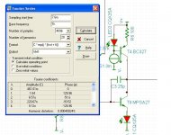
As bcarso pointed out, this is more about the caps increasing the errors in your simulation results, than about actual distortion. For a 1KHz test, I'd run the simulation for 10mS, and only do the Fourier analysis on the 2'nd half. Bcarso's approach is more extreme, but the idea's the same: allow a bit of time for the circuit to settle after applying the input signal before starting the measurement, then do the analysis over several cycles. Another important thing for accurate results is to use a small timestep. For testing at 1KHz, I'd set the maximum timestep to 1uS. Smaller timesteps for higher frequencies.Every time I added a capacitor, distortion got worse, sometimes much worse. I reduced the Miller capacitor and distortion goes down. I eliminate the bypass cap in the feedback network, distortion goes way down. What's even more curious to me is that adding an RC RF LP filter at the input causes distortion also.
Fun times ahead.jfet's used as CCS's.

As I understand it, jfet parameters vary wildly from device to device, so you may have to measure the individual fets and select the resistors accordingly.
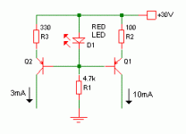
I'm way too lazy for that and would rather do it the easy way e.g. as shown below. The forward voltage on an ordinary red LED is about 1.7V, so there's about 1V across the emitter resistors, which makes the arithmetic easy.
If you have rail voltage to spare, it might be better to replace the LED with a 6.8V zener. That would give better compliance, but maybe a bit more noise.
Attachments
As bcarso pointed out, this is more about the caps increasing the errors in your simulation results, than about actual distortion. For a 1KHz test, I'd run the simulation for 10mS, and only do the Fourier analysis on the 2'nd half. Bcarso's approach is more extreme, but the idea's the same: allow a bit of time for the circuit to settle after applying the input signal before starting the measurement, then do the analysis over several cycles. Another important thing for accurate results is to use a small timestep. For testing at 1KHz, I'd set the maximum timestep to 1uS. Smaller timesteps for higher frequencies.
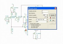
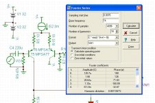
I don't think I have these options. See the attached screen shot.
Attachments
Fun times ahead.
As I understand it, jfet parameters vary wildly from device to device, so you may have to measure the individual fets and select the resistors accordingly.
I'm way too lazy for that and would rather do it the easy way e.g. as shown below. The forward voltage on an ordinary red LED is about 1.7V, so there's about 1V across the emitter resistors, which makes the arithmetic easy.
If you have rail voltage to spare, it might be better to replace the LED with a 6.8V zener. That would give better compliance, but maybe a bit more noise.
Thanks! Great idea!
Are these more linear than current regulating diodes?
I'm not convinced the added complication of a diamond buffer is worth it. I'd maybe use a simple 2 transistor buffer to increase output current capability, but that's it.
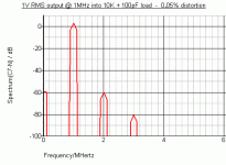
Out of curiosity, I simmed a simple circuit with no buffer and got pretty decent results. Distortion at 2V pk-pk output into a 10K load looks like about 4ppm @ 1KHz, and 30ppm at 20KHz. It's mostly 2'nd harmonic too; everything else is far down.
I did notice that a small cap across the feedback resistor is needed for good stability, mostly to ensure that the base of Q2 is driven from a low impedance at high frequencies. Also note that heavy degeneration of the input pair allows good stability with a small Miller cap.
Disclaimer: real world performance is likely to be different to the simulator results since the spice transistor models aren't likely to be very accurate.
P.S. The 10m caps in the circuit are artificially high just to reduce simulator errors.
Attachments
Hmm... Looks like you can at least set the "sampling start time" to 5 or 10 mS. That might help. Getting rid if coupling caps, or using huge values also helps a lot. e.g. the 10000uF caps in the circuit I just posted.I don't think I have these options. See the attached screen shot.
Are these more linear than current regulating diodes?
No idea. If you're really bored you could pore over the datasheets, and compare with simmed results for discrete CCS. I've never actually seen them used in a circuit though. I presume if they were any good, they'd be more popular?
A good question as to why they are not more popular. Jung has been doing a lot of investigation of current sources lately, and I don't want to violate confidential comms before he publishes. But he does like roll-your-own cascaded depletion-mode DMOS, the ones from Supertex, although I note that they come with quite a voltage burden. They are pretty quiet despite being MOS, and they come with their built-in reference voltage as it were.
The Vishay app note on CC "diodes" shows cascaded JFETs as an option, but then talks about their available CC parts, and based upon how little voltage across is required to start getting high Z, I infer that none of the commercial two-terminal parts have an actual cascade inside (or "cascode" if one prefer).
For this circuit, with this sort of loading (almost nothing) on the second stage output by the diamond buffer, and given the output-Z-reducing effects of the cap feedback around the second stage at mid-high frequencies, the 10mA source's output Z may not be too critical --- very high output resistance will improve low-frequency gain, but that (a) may not do anything for the audio performance and (b) will ultimately be limited by the collector impedance of the second stage transistor, which isn't all that high at low frequencies. If we migrate to a simpler complementary e-follower output buffer the effect of lower impedance at its input will be now more load-dependent. Many are the tradeoffs.
But again, I guess it's been feasible for our intrepid experimenter to append the diamond stage, while tearups to the preceding sections are evidently less palatable. Were that not the case I could see repurposing the same bag of transistors (input stage I mirror, additional transistor in the second stage, yada yada). I'm frankly surprised by how good the predicted performance is with this simple a second stage; despite significant effects being neglected, it actually looks like some pretty decent performance can be achieved. But we are spending a lot of power to get here, and we still need to source some higher voltage transistors (not a big problem, and I doubt the results will change that much).
With +-20V rails, the transistors can't get more than Vce max across them. I also dropped the 2'nd stage idling current to get the device dissipation down to about 100mW. Seemed prudent. With that approach, the existing transistors should be OK. I see the goal here as making the most of the PCB and components that came with the kit....despite significant effects being neglected, it actually looks like some pretty decent performance can be achieved. But we are spending a lot of power to get here, and we still need to source some higher voltage transistors (not a big problem, and I doubt the results will change that much).
Half the reason I did the sim above is that, IIRC, the OP never simmed the original circuit before going to town with the mods. So it was sort of a "back to the roots" exercise, sticking as close as possible to the original (except for the CCSs - the original biasing scheme deserves to be taken out and shot
).Edit:
I just tried the sim again, but changed the transistors to Bob Cordell's models for 2n3904 and 2n3906 (i.e. good models of bad transistors). Distortion remained about the same at 20KHz and only got about 3 times worse at 1KHz. That's encouraging.
Last edited:
(i.e. good models of bad transistors)
Amen. And I can still remember when those were considered good parts.
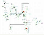
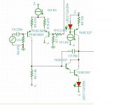
Adding the diamond buffer seems to drop the distortion about 10 times (0.02% vs. 0.002%, 1kHz, 1Vp-p), given the same values for the LTP and VAS in each of them. Fourier analyzer was delayed by 0.0076 sec. I left the buffer untouched. The CRD's have internal impedances of 1M ohm. The current in the VAS is about 7.5mA. I increased degeneration in the LTP as suggested. CRD's fit on the board much better than discrete components. Bandwidth is good with nice smooth roll off above 1MHz with no funny stuff. There is no phase shift in the audio range. I believe these transistors are current production so this could be built with them instead of using the originals, which are 2SA1015 in the LTP, 2SD667 for the VAS, and 2SB647 for the CCS. I did buy those already though.
Thanks!
Thanks!
Attachments
Last edited:
Used as a voltage reference, effectively a 1.7V Zener, but with lower noise.
I am referring to LED1.
Why? It lets you raise the LTP load resistor for a notional open loop gain, but you could do much better by going for a beta enhancer.
The LTP degen resistors are not ideal for low noise. Better to use a comp cap from VAS output to inverting input.
Seems 3 steps forward and then 2 back . . . And the fundamentals are still not all in place.
Last edited:
I am referring to LED1.
Why? It lets you raise the LTP load resistor for a notional open loop gain, but you could do much better by going for a beta enhancer.
The LTP degen resistors are not ideal for low noise. Better to use a comp cap from VAS output to inverting input.
Seems 3 steps forward and then 2 back . . . And the fundamentals are still not all in place.
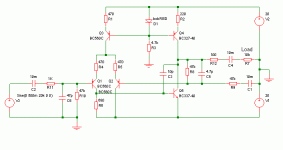
I have to work within the limitations of the boards I bought. That's why things are much more simple than maybe you'd like to see. See the schematic in the first post. I can do things like use SMD chip resistors in place of the trim pot in the LTP, for example, but drilling more holes and cutting traces is not something I want to do. Granted, this is a lot of effort for boards that don't cost very much, but it's more interesting as a challenge to work within certain confines like the board layout.
I added another BC337 to make a Darlington pair in the VAS. Distortion was cut in half to 0.001%, in the circuit with the buffer. I adjusted the load resistor for the LTP to get the DC balance correct. VAS current remains the same at 7.5mA. I guess this is sort of a "beta enhancer" from a search in Google, though I didn't see this specific topology there. I can get Darlington transistors as 3 legged critters so this would fit on the board.
Thanks for the suggestion!
The LTP is so non-linear that I believe a lot of degeneration is required there in spite of the noise problem.
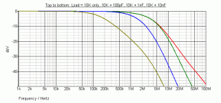
Bandwidth is good with a nice smooth rolloff above 1MHz.
I feel blessed to have so much wise help here! I'm learning so fast my brain is about to explode!
Thanks for the suggestion!
The LTP is so non-linear that I believe a lot of degeneration is required there in spite of the noise problem.
Bandwidth is good with a nice smooth rolloff above 1MHz.
I feel blessed to have so much wise help here! I'm learning so fast my brain is about to explode!
Attachments
Last edited:
That circuit should work a lot better with 2 little changes:I added another BC337 to make a Darlington pair in the VAS.
A) Connect the collector of T9 to ground, rather than to the collector of T3, so you don't have T9's nonlinear collector-base capacitance in parallel with C3.
B) Connect a resistor (1K to 2K?) between the emitter of T9 and the negative supply rail, so that there is always 1 or 2mA of current flowing through T9.
So, I got a little crazy here. I replaced the input pair with PNP Darlington transistors, the MPSA77, which is now End of Life unfortunately. I reduced the degeneration resistors to 10 ohms. Distortion is now 0.0017% with no buffer. Dang. I'm impressed. Bandwidth is still good up to about 1MHz.
Attachments
That circuit should work a lot better with 2 little changes:
A) Connect the collector of T9 to ground, rather than to the collector of T3, so you don't have T9's nonlinear collector-base capacitance in parallel with C3.
B) Connect a resistor (1K to 2K?) between the emitter of T9 and the negative supply rail, so that there is always 1 or 2mA of current flowing through T9.
Thanks but I don't think I have room on the board to make these changes, even if I use SMD's.
- Status
- This old topic is closed. If you want to reopen this topic, contact a moderator using the "Report Post" button.
- Home
- Source & Line
- Analog Line Level
- discrete op amp