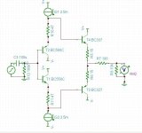
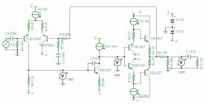
So I was fooling around with the buffer and got this one set up with +/-15vDC supplies. Distortion is 1.3x10^-5 (0.0000129%).
The reason I did this was because I have another circuit board that has an IC opamp with diamond buffer and I wanted to see if the components had been optimized.
Then I realized I had misread the schematic. So I corrected it, but the distortion isn't much different (0.0000136%). I don't see any advantage to the second version.
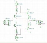
Attachments
Have some good and cheap kits, perhaps are the best choice:
Classic Audio Products of Illinois
Classic Audio Products of Illinois
Happy days, Raúl Couto
Thanks. Those look good.
Fascinating thread to join late and follow the evolution! It's also interesting to see how much we're treating Simland as reality.
Most all of the suggestions have been excellent and have helped the circuit evolve to something fairly decent. One remark a bit back that needs addressing: when the overall loop is closed, you should expect the distortions measured within the loop with your (presumably high-Z) simulation voltmeter to be highish, given all the nonlinearities that global feedback is correcting. This is a good sign, not a sucky one.
Another remark that passed unnoticed (or I missed it): the noise at the input should be dominated by the source impedance, given a sufficiently large coupling cap, unless this source Z is very high (and it's probably not). Making the input resistor smaller will reduce gain by loading the source component, and the net result will be poorer. Resistor thermal noise is not some voltage source that imposes its level across anything to which it's connected --- the voltage noise generator is in series with the resistor. It is true that when the coupling cap Z gets large at low frequencies you will start to see more base current noise effects, but this should properly be mostly infrasonic.
So noting that, although you are (I hope) planning on a.c. coupling at the output to your sub amp as well as retaining the input coupling cap to your source, if low d.c. offset is desired the practice is to have the d.c. resistance seen at each base of the LTP the same. Since on the right you have 33k, best practice (absent other considerations) would be to make the input termination resistor the same value.
What a great learning experience! Coming from a background of tubes I trust you're nonetheless aware of the unforgiving nature of sand-state. Component failures are very easy to induce with a slip of a probe, and you don't have the warning of even much of a spark most of the time, let alone noticing the plates of tubes glowing cherry-red
Brad
Thanks for all your kind word Brad. I wasn't aware that resistor noise was in series with the resistor and not in parallel. So, I suppose this means that I don't have to be concerned about having a large value resistor bewteen the input and ground. Thanks!
I tried replacing the input pair with P channel jfets, but it didn't help at all. I rebalanced the circuit of course. The bipolars have lower distortion in this circuit.
I'm going to open the feed back loop and see if I can optimize the circuit that way.
Your VAS current souce is not set up correctly - Godfrey pointed you in the right direction. As it stands now, your VAS is not current source loaded. At this stage, its better to just replace T4 with a current source and re-run your sims.
Same story for the VAS emitter resistor - its too high and you are likely losing a lot of loop gain as a result.
Keep going. With this topoloigy you can get a lot better than the 50ppm you are seeing now.
Really? what's wrong with the constant current load on the VAS? It seems to be textbook to me. I'll replace T4 with a current source and see what's up.
I adjust the VAS emitter resistor to produce the lowest distortion with the Fourier analyzer, but I'm going to try this with the feedback loop open.
Be careful with that. In the simulator, you're using perfect constant current sources. In the real world, "constant current diodes" are anything but perfect. The current can vary quite a bit with voltage, in a nonlinear way, so they may actually add distortion.
Disclaimer: I've never actually used them, just looked at a random datasheet yesterday to see if they're any good. Seems some are much better (or worse) than others.
but bear in mind that this is already excellent performance compared to most commercial gear.
I set the internal impedance of the current sources to 1Mohm. I realize that in the real world CRD's are not perfect. The flatness of the current output with voltage depends on the current rating for the device, with higher current ones worse than lower current ones.
Without the feedback loop in place, with the feedback network removed and replaced with one resistor to ground, as well as replacing T4 with a current source, I'm getting something like 37% distortion, even with equal currents flowing through the LTP transistors. The gain is huge after the VAS, but I can't seem to get the output from VAS better than about 3voltsDC. I adjusted the current source for the VAS down to 3mA, from 5.94mA in the original design. I separated the buffer from the rest of it also, since it's the first two stages that are causing problems. The buffer is really good.
I think the voltmeter in Tina probably have infinite impedance. There's no control for that though.
I'm feeling frustrated with it right now.
Attachments
I was looking at e circuit in post 77. This is not ideal.
When you tweak he vas emitter resistor, check out the LTP current balance and let us know what happens.
Yeah, they are interrelated. I can't change one without changing the other. Every time I change the VAS emitter resistor, I have to change the load resistor as well to balance the LTP.
Thanks for all your kind word Brad. I wasn't aware that resistor noise was in series with the resistor and not in parallel. So, I suppose this means that I don't have to be concerned about having a large value resistor bewteen the input and ground. Thanks!
I tried replacing the input pair with P channel jfets, but it didn't help at all. I rebalanced the circuit of course. The bipolars have lower distortion in this circuit.
I'm going to open the feed back loop and see if I can optimize the circuit that way.
There are two equivalent models for resistor thermal noise. One consists of a voltage noise in series, the other a current noise in parallel. Each model gives the same circuit result, but one is often more suitable for calculation than the other. Where a lot of folks go wrong is to suppose that the open-circuit voltage noise is like a voltage generator, which leads to the result that the lower the resistance the better, regardless of what the rest of the circuit looks like.
P channel JFETs are generally higher capacitance for the same transconductance compared to N channel, as the mobility of holes in silicon is quite a bit lower than that of electrons. It's also fairly hard to find good ones these days, the Toshiba 2SJ109 duals being long gone. And those old parts (the N channel version being the 2SK389) have a rapid rise in gate leakage with drain-gate voltage which can spoil things sometimes. So they are often helped along with cascaded bipolars or other JFETs, which can give excellent results at higher cost and complexity. I think you're fine with decent bipolars in this application.
I think you were on the right track with your penultimate revision, before you took out the emitter resistors in the diff pair --- that last complete amp circuit looked unstable. although I didn't verify that in sim. I did do a bit of playing around with compensation on a slightly modified penultimate one (we should probably have rev numbers to identify) and got some promising results, from experience mostly "sweet Spice lies" as they neglect various effects like signal-induced self-heating and voltage breakdown, but of interest nonetheless. If time permits I'll publish them here.
I know the transistors migrated to ones that were in your library, and that's fine for openers. Be aware though that their abs max ratings are potentially exceeded in some locations, both in terms of voltages and power dissipation. The output stage in particular is running at quite a rich bias, which looks great for distortion but will likely break in real life.
Remarks about the constant current diodes from Godfrey are astute. Internally they are JFETs with resistors in the source and the gate tied to the resistor free end. These are wildly different in efficacy. They also have their own limitations in terms of voltage withstand and power dissipation, and as remarked have less-than-perfect (i.e., infinite) impedance which is moreover voltage dependent. I'm not saying don't use them, just be aware that if Spice is using perfect current sources your mileage will vary.
Other parameters of an opamp will also be apparent in the so-called real world. One already came up, when the second stage PNP source was referenced to the negative rail rather than (as now) referenced to the positive one, which as noted led to a horrendous modulation of the current by any rail fluctuations. Again Spice was set up to have perfect power supplies, so we can hardly fault it
") Eventually one sets up rail disturbances and sees how much the amp responds to them (i.e., you evaluate PSRR, power supply rejection ratio).
Eventually one sets up rail disturbances and sees how much the amp responds to them (i.e., you evaluate PSRR, power supply rejection ratio). Anyway, again this is a great educational opportunity, and these tools are such an advance compared to olden days. However, it's a little bit like learning to drive with a Ferrari, except that fortunately it's a Ferrari simulator. As usual there is no substitute for the real thing, or for good circuit understanding and insight. Your tube experience is a good start (I liked your description of the input termination as being "self-bias", even though the physics involved is completely different). Be patient if you can.
Oh---the open loop study is worthwhile, particularly giving attention to phase. For feedback the typical rule-of-thumb is to have loop gain be unity while there is still a ~45 degree margin left before negative feedback becomes positive (almost-guaranteed oscillation). Typically the open-loop gain will be flat at low frequencies, enter a region of about 90 degrees phase shift, then start nosing down towards 180 and oblivion. There are probably some good wikis about all of this.
Note as well that the input capacitance of the negative input transistor interacts with the feedback to produce another unwanted pole pair. Think of the feedback capacitor, initially at least, as a way of reducing that effect. Having the collector of that side of the diff pair tied to the negative rail helps here by avoiding voltage swing beyond just that due to tracking the input voltage --- e.g., the "Miller" effect multiplier is just unity. Also the relatively high voltage reduces the collector-base capacitance as well. So for the input C compensation per se, you shouldn't need much --- a couple pFs. But if you try to set your closed-loop bandwidth via that part, you have other effects, and if the amplifier is not unity-gain stable you may invite oscillations.
Brad
Thanks again Brad! Give me some time to digest your very insightful comments. I can't tell you how much I appreciate yours and everyone's help with this.
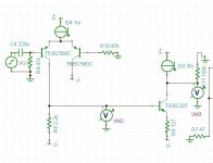
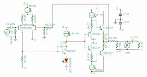
I figured out a serious problem with this circuit. The input impedance to the VAS is way too low for the LTP to drive. The only way I know how to raise the input impedance of T3 is to add the stopper resistor. I started at 47ohms and kept running the Fourier analyzer. The input stage @ VM2 is produce 0.9% distortion with no global feedback. This is a reduction from some 30% before.
Is there another way to increase the input impedance of the VAS. I suppose I could change T3 to a JFET, that would do it I think, but there's probably other ways to do it.
I'm happy I found this problem. Now the VAS needs to be optimized because it's producing a lot of distortion. Later, I have other things that need doing.
Thanks again for the support! much appreciated!
Attachments
[snip]
I figured out a serious problem with this circuit. The input impedance to the VAS is way too low for the LTP to drive. The only way I know how to raise the input impedance of T3 is to add the stopper resistor. I started at 47ohms and kept running the Fourier analyzer. The input stage @ VM2 is produce 0.9% distortion with no global feedback. This is a reduction from some 30% before.
Is there another way to increase the input impedance of the VAS. I suppose I could change T3 to a JFET, that would do it I think, but there's probably other ways to do it.
I'm happy I found this problem. Now the VAS needs to be optimized because it's producing a lot of distortion. Later, I have other things that need doing.
Thanks again for the support! much appreciated!
The function of the second stage* is typically to act as a dominant pole response for the overall amp response, and the typical feedback capacitor from input to collecting electrode makes the input impedance of the stage look low. But that's not a bad thing; rather, the input stage looks like a high Z output anyway, i.e. like roughly itself a current source. So you have input stage transconductance (so many amps per so many differential volts) driving a current into another transconductance with capacitative feedback (second stage transistor), output of which is a voltage roughly proportional to the negative time integral of the input current. So the effect of that capacitor at higher frequencies is to both lower input Z and lower output Z, in accord with how "shunt feedback" works. Then you have your diamond buffer which transforms the output load and feedback/feedback divider load to a much higher impedance at the output of the second stage. And then close the loop around the whole works and you're done
Nothing wrong with making the second stage have lower distortion though, and the cap feedback also reduces it from the open loop value. Typically the existing device is prefaced with another, usually an emitter follower of the same polarity whose collector is tied high (ground suffices, with a bit of R in series to protect against excessive base current into the output device).
Having said all that, someone pointed out that the emitter resistor for that second stage device is fairly large, which limits the equivalent transconductance. However, it can still be used as is, and provides a d.c. offset above the negative rail which facilitates adding a more complex circuit ahead of it (like a current mirror, so you can do something with the output current of that other transistor of the differential pair). And by paralleling some additional series R-C across that emitter R you can extend the phase margin usefully (see the Jensen 990 approach for example iirc).
You could also (if the elevation above the neg rail becomes of interest) use an LED in series in place of the resistor, which has roughly the impedance of a forward biased normal Si diode with an additional voltage drop. Many are the ways
Brad
*which Bruno Putzeys protests [see his Linear Audio article "The F-Word" to which I believe Jan Didden has provided a free link in another thread in here] should not be called a VAS; but I'm afraid just about everybody has settled into that convention; perhaps it should be called "the first high output-voltage-swing stage". Yeah VAS is probably here to stay.
R16 is a no-no. You are curing symtoms here and not the cause. There is also the noise issue that makes this the wrong thing to do.
Your LTP current is 500uA per side. If you are insistent on having R6 and IS3 is set to 3mA then pick a voltage drop across R6 that you would like to see - lets say 1V for arguments sake. 3mA and a 1V drop comes out at 330 Ohms for R6. Now for the LTP to be nominally balanced, the base of T3 will have to sit at 1V+0.6V - so 1.6V above the -ve rail. 500uA needs R8 to be at 3200 ohms. Ditch R16 - you do not need it.
In your current set up above, you are not buffering the VAS and you have no feedback (Cdom and global loop). I would put your diamond buffer back in and Cdom and see what you get. Its too early to go delving into the circuit open loop to try to reduce distortion.
Once you have the basic circuit running, there are a few other tricks which will make a significant improvement - like a beta enhancer for example, and a current mirror LTP load.
Also, you need to be testing this circuit at 20KHz and at 10V output so that you exercise it fully, and the distortion is down in the single digits ppm level. Then you can be sure that at 1-2 volts out, you will be in the sub ppm level.
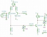
OK, thanks for the information everyone. This circuit has 0.004% distortion at 1Vp-p input, 20kHz. I found that I needed to juice up the VAS substantially to reduce distortion. I increased the current in the LTP as well.
Please note that I don't have the frequency compensation finished on this circuit yet. As it stands now, it has a resonance at about 2.8MHz. It's unfortunate that I can't use the resistor between the LTP and the VAS like in previous iterations of this circuit because it forms a nice filter with the Miller capacitor to give a nice roll off at some 600KHz, depending on the relative values for the resistor and capacitor of course.
Please note that I don't have the frequency compensation finished on this circuit yet. As it stands now, it has a resonance at about 2.8MHz. It's unfortunate that I can't use the resistor between the LTP and the VAS like in previous iterations of this circuit because it forms a nice filter with the Miller capacitor to give a nice roll off at some 600KHz, depending on the relative values for the resistor and capacitor of course.
Attachments
Last edited:
Once you have the basic circuit running, there are a few other tricks which will make a significant improvement - like a beta enhancer for example, and a current mirror LTP load.
Also, you need to be testing this circuit at 20KHz and at 10V output so that you exercise it fully, and the distortion is down in the single digits ppm level. Then you can be sure that at 1-2 volts out, you will be in the sub ppm level.
Thanks for your suggestions. I've made some changes to the circuit.
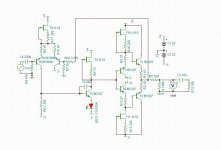
I don't know what is a beta enhancer, but I do know that I can't add a current mirror to the LTP without abandoning the existing circuit boards. I probably wouldn't be doing this circuit if I was starting from scratch. What I'm doing is trying to work within the limitations of the existing circuit boards, as shown in the schematic of my first post on this thread.
The function of the second stage* is typically to act as a dominant pole response for the overall amp response, and the typical feedback capacitor from input to collecting electrode makes the input impedance of the stage look low. But that's not a bad thing; rather, the input stage looks like a high Z output anyway, i.e. like roughly itself a current source. So you have input stage transconductance (so many amps per so many differential volts) driving a current into another transconductance with capacitative feedback (second stage transistor), output of which is a voltage roughly proportional to the negative time integral of the input current. So the effect of that capacitor at higher frequencies is to both lower input Z and lower output Z, in accord with how "shunt feedback" works. Then you have your diamond buffer which transforms the output load and feedback/feedback divider load to a much higher impedance at the output of the second stage. And then close the loop around the whole works and you're done
Nothing wrong with making the second stage have lower distortion though, and the cap feedback also reduces it from the open loop value. Typically the existing device is prefaced with another, usually an emitter follower of the same polarity whose collector is tied high (ground suffices, with a bit of R in series to protect against excessive base current into the output device).
Having said all that, someone pointed out that the emitter resistor for that second stage device is fairly large, which limits the equivalent transconductance. However, it can still be used as is, and provides a d.c. offset above the negative rail which facilitates adding a more complex circuit ahead of it (like a current mirror, so you can do something with the output current of that other transistor of the differential pair). And by paralleling some additional series R-C across that emitter R you can extend the phase margin usefully (see the Jensen 990 approach for example iirc).
You could also (if the elevation above the neg rail becomes of interest) use an LED in series in place of the resistor, which has roughly the impedance of a forward biased normal Si diode with an additional voltage drop. Many are the ways
Brad
*which Bruno Putzeys protests [see his Linear Audio article "The F-Word" to which I believe Jan Didden has provided a free link in another thread in here] should not be called a VAS; but I'm afraid just about everybody has settled into that convention; perhaps it should be called "the first high output-voltage-swing stage". Yeah VAS is probably here to stay.
Thanks again for the suggestions Brad. Very helpful as always. I can see that the original circuit boards I have are very limited. I've made some changes to the circuit now. The original currents through the LTP and the VAS were based on the original parts specifications. I have since learned that I needed to juice up the VAS substantially, as well as adding more current to the LTP.
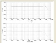
Does anyone know how to compensate a differential amplifier to kill this resonance? As you can see, both the gain and phase response are pretty bad, with a strong resonance at 3MHz. This is the output at VM2.
Maybe I'm looking at the error signal, I don't know.
Does anyone know how to compensate a differential amplifier to kill this resonance? As you can see, both the gain and phase response are pretty bad, with a strong resonance at 3MHz. This is the output at VM2.
You are still approaching this as if it were an open-loop circuit and not looking as Peter O'Toole says in Creator, at the "Big Picture"
What we're interested in at least to begin with is what the overall amplifier response is. And yes, the closed loop response now has some output peaking before rolloff, not severe but probably curable with a little cap across the feedback resistor.
At risk of getting tied to this more than may be warranted, I'm attaching a pdf of something to suggest a few changes that still should be accessible without a big tearup --- as that is one of your constraints.
Since we're burning power here, we can profitably reduce the impedance of the feedback network for smaller effects due to the negative input's characteristics. I took things down a bunch, and I've not shown input and feedback divider caps since they slow settling for simulations. However, the feedback divider one should get proportionally larger to preserve the low frequency cutoff. That may mean a big cap. Alternatively, if the circuit you are driving already has a d.c. block, you might just want to run d.c.-coupled.
I added the LED so as to provide a higher voltage at the second stage and thus permit a larger R (your 1.1k R8 becomes 1.65k), and returned the collector of your T6 to the LED. This has a miniscule effect by providing a little additional loop gain, but it does no harm, and by increasing the LED bias current reduces its impedance a bit (for the model of standard red LED my simulator uses, the impedance thus is around 9 ohms). So we help loop gain by having an emitter R of 9 ohms instead of 86, and our integrator is more accurate. Another advantage of the collector return thus is that now the dissipation change for large signals in each half of the input pair tend to almost exactly track, reducing thermal distortions (which most simulators emphatically do not model, and can be one of the sweet Spice lie spoilers). This concern is a little academic since the dissipation of the second stage device fluctuates wildly, as will whatever you use for the 10mA current source. But it does no harm. There is unfortunately a larger temperature coefficient of second stage input voltage, which could be addressed in various ways. Also, when the transistor heats up as it very much will, its base-emitter voltage will be less --- so for the balance of currents in the diff pair, your resistor R8 will tend to get smaller.
I also put in a more realistic 1k as a source impedance, rather than just your C4 driven from a voltage source.
The predicted frequency response closed-loop is nicely flat and about 3dB down from midband at around 8MHz, which isn't too shabby. The slew rate should be good albeit asymmetrical for very fast signals. It will be prudent to put a little passive lowpass at the input if you're likely to have absurdly out-of-band signals.
And again, warnings as before about dissipation in things after the diff pair, although you have toned down the diamond stage bias now without any other ill effects evident.
Attachments
Thanks so much! Great suggestions!
It seems that for distortion, less capacitors is much better. This circuit has 0.0005% @ 1kHz, 1Vp-p input, and 0.007% @ 20kHz. Source impedance is 600ohms. Every time I added a capacitor, distortion got worse, sometimes much worse. I reduced the Miller capacitor and distortion goes down. I eliminate the bypass cap in the feedback network, distortion goes way down. What's even more curious to me is that adding an RC RF LP filter at the input causes distortion also.
I had set the feedback resistor to a high value because I was told it had to be the same value as the input resistor, since the LTP is self biased. But, it seems to work great with the low values in the feedback network. Since it's driven by the buffer then low values should be no problem.
The dB and phase response are attached as well, with -3dB @ about 12MHz. I suppose I could put this into a box and use feedthru capacitors....
Thanks again, this is great!
Attachments
Thanks so much! Great suggestions!
It seems that for distortion, less capacitors is much better. This circuit has 0.0005% @ 1kHz, 1Vp-p input, and 0.007% @ 20kHz. Source impedance is 600ohms. Every time I added a capacitor, distortion got worse, sometimes much worse. I reduced the Miller capacitor and distortion goes down. I eliminate the bypass cap in the feedback network, distortion goes way down. What's even more curious to me is that adding an RC RF LP filter at the input causes distortion also.
I had set the feedback resistor to a high value because I was told it had to be the same value as the input resistor, since the LTP is self biased. But, it seems to work great with the low values in the feedback network. Since it's driven by the buffer then low values should be no problem.
The dB and phase response are attached as well, with -3dB @ about 12MHz. I suppose I could put this into a box and use feedthru capacitors....
Thanks again, this is great!
The input devices require a source for their base currents, which for matched devices at balance should be the same. IF d.c. accuracy is important the practice is to have each device see the same external resistance. A lot of inverting-mode opamp circuits show a resistor in the noninverting input to ground, and assume that one is concerned about minimizing offset voltage due to input bias currents --- sometimes people don't realize why that resistor is there and add it as a matter of course, even when bias current is negligible (FET input amps for example), and then all it does is add noise.
But if you can tolerate some d.c. offset (and almost surely the destination device is a.c.-coupled), at these gains there's no harm in unequal impedances at each input. And having a lower impedance for the feedback clearly helps us.
Beware of assuming that the simulator is telling the truth if you get strange results with capacitors however. Try changing the simulation time (say, run for 100ms and look at the data after 90ms, so the plot routine doesn't go crazy from too many points to plot) and see if you get the same answer. I'm impatient, so wherever possible I d.c.-couple. The input filter adding distortion is in particular very suspicious, as that should settle very quickly. BTW, in my sim the slew rate is good enough to tolerate large input signals with rise and fall times of 50ns without overshoot, and shows the slew rates to be about 28V/us and still pretty symmetrical, which is quite decent and more than enough for about anything audio sources will throw at it.
When looking at open-loop response, with very high low-frequency gain you may still have to wait a long time for things to settle. Samuel Groner often uses a gigantic feedback inductor in sim to provide d.c. feedback, but still allowing the rest of the response to show. My simulator often balks at this approach but it's a nice strategy otherwise.
Next step for you should be to put in real current sources. Note that for the ideal ones in my sim the rather large signal output shown occurs at a very low distortion, and that's looking at harmonics out to 23kHz. Second harmonic is still dominant at the level shown, although 3rd is climbing as one expects.
- Status
- This old topic is closed. If you want to reopen this topic, contact a moderator using the "Report Post" button.
- Home
- Source & Line
- Analog Line Level
- discrete op amp