You can get a nice clean download of the TNT 200 schematic with the parts list from this site, for anyone who may be interested.
Thanks very much, Ian.
Cheers,
Bob
Considering e.g. the phase plot in Figure 9.5 on page 179 of your book, I would not be surprised if the versions with and without bridge cap would show different ringing behaviour. Even if a very good input filter is in place, we have to keep in mind that it is impossible in practice to keep high frequency excitations away from the amplifier: distortion residuals, power supply noise, etc. So, if there is a possibility to ring, the circuit will do it.
Some years ago, I tried to bring an own amplifier to the market. When presenting a certain version of a design to different dealers, I was always astonished how consistent their remarks on strenghts and weaknesses of the sound of this particular version have been. Since that time I recognise that there is virtually nothing that connot be heard.
Best regards,
Matthias
Hi matze,
This is a good observation. I'll try to take a look at ringing behavior at various nodes in TPC and BTPC.
Your remarks about subjective comparisons and comments from different people is very interesting, even though it is not exactly a single or double-blind test. Is there any chance that you brought two different versions of the amplifiers to these people and they listened to both?
Maybe yours was very clean and neutral, and they were not used to listening to such an amplifier
") .
.Cheers,
Bob
Hi kgrlee,
Thanks for bringing this to my attention. Is this sort of like the "tail wags the dog" where we have essentially a conventional topology where the conventional output goes to ground and the signal appears on the floating power supply? Something like Crown uses in some of their amps?
I'd like to get a hold of that 1997 EW paper if possible, so I can get a better understanding of it.
It may very well be a topology worth some discussion in the next edition.
Cheers,
Bob
Hi Bob,
If you're going to write about the common emitter/common source output stage topology, I would suggest you consult Cherry's paper on the subject and Dr Stephen Gift's objections to the breed. Both of these are AES papers:
"Feedback amplifier output stages" by Stephen J. G. Gift
"Comments on feedback amplifier output stages" by Edward M. Cherry and Gregory K. Cambrell
"Authors reply"-Stephen J. G. Gift
all in JAES Volume 33, No. 10, 1985 October
Last edited:
Hi forr,
If I read it right, this Acoustat does look like the "tail wags the dog" topology. Am I right? Thanks for putting this up.
Interesting, looks like they used MOSFETs for the input LTP.
Could you send me an electronic copy of this schematic so that I can see the details more clearly?
Cheers,
Bob
Hi Bob,
I sent you the AUDIO magazine March 1983 full article, which showed the schematics, and the patents by its author.
(anybody else wanting it, send me an MP mentionning your email).
The circuit was invented by James Strickland and was patended, # 4467288.
What is very curious with this design is the feedback scheme
from which a very high damping factor is obtained.
The same kind of ouput stage was used by Hafler which bought Transnova, however the feedback scheme was more usual.
Regards.
This is true. The only thing missing is an explanation in respect of why you and Bob consider it necessary to split the coincident poles.
In my view the resonant peak is completely innocuous: there is no need to reduce loop transmission by splitting the coincident poles.
I haven't done enough research to advocate one way or another. I simply provide readers of my paper with a way in which they can split the poles, should they so desire.
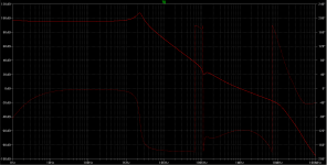
The thing that concerns me is not the peak per se. The higher the Q of the complex poles (if they are complex at all), the more rapid the transition of loop-gain phase from 0 degrees towards -180 degrees. Depending on the location of the compensation zero, loop gain phase can go within a degree or two of -180. Complex loads (particularly highly capacitive ones) on the amplifier output can knock this over the -180 degree barrier. Of course, the phase recovers whilst the loop gain is still greater than unity so the system is stable - conditionally. See below an example loop gain bode plot of a TPC compensated amplifier with an 8 R || 2 uF load.
It is this conditional stability that gives me cause for concern and requires further investigation.
Attachments
Last edited:
A correctly designed TPC amplifier will not be conditionayl stable unless you're operating it at unity gain, i.e. 100% loop gain. However, this condition does not arise with ordinary power amplifiers.
And, yes, they're complex poles if you have a relatively large amount of current gain within the minor loop.
And, yes, they're complex poles if you have a relatively large amount of current gain within the minor loop.
Last edited:
Common emitter output stage
This amp was published by Wim de Jager in british Electronics World, December 1999.
Low maximum slew-rate but good thermal stability according to Francis Brooke's simulations :
( https://sites.google.com/site/francisaudio69/6-l-amplificateur/6-1-comment-simuler-un-amplificateur )
[ in french ]
An externally hosted image should be here but it was not working when we last tested it.
This amp was published by Wim de Jager in british Electronics World, December 1999.
Low maximum slew-rate but good thermal stability according to Francis Brooke's simulations :
( https://sites.google.com/site/francisaudio69/6-l-amplificateur/6-1-comment-simuler-un-amplificateur )
[ in french ]
Last edited:
Harry, I did a lot of this 'linear' analysis on TPC type topologies circa 1990.The thing that concerns me is not the peak per se. The higher the Q of the complex poles (if they are complex at all), the more rapid the transition of loop-gain phase from 0 degrees towards -180 degrees. Depending on the location of the compensation zero, loop gain phase can go within a degree or two of -180. Complex loads (particularly highly capacitive ones) on the amplifier output can knock this over the -180 degree barrier. Of course, the phase recovers whilst the loop gain is still greater than unity so the system is stable - conditionally. See below an example loop gain bode plot of a TPC compensated amplifier with an 8 R || 2 uF load.
It is this conditional stability that gives me cause for concern and requires further investigation.
Can you show us a Close Loop response, either .AC or .TRANS which exhibits problems with
- sensible gains, conditions & loads (loads can be stupid)
- stupid gains, conditions & load eg unity gain?
A correctly designed TPC amplifier will not be conditionayl stable unless you're operating it at unity gain, i.e. 100% loop gain.
The amplifier whose loop gain response is depicted has a closed-loop gain of 26 dB. When loaded with a purely resistive 8R load, it has a phase margin of 62° and a gain margin of 17.2 dB. In what way is this not (as you have insinuated) "correctly designed"?
There's something very wrong with your amplifier as, from the loop gain response, it appear to have a notch at 100KHz which really wreaks havoc with the phase response.
I have never seen a TPC amplifier with such a loop gain response.
I said, that happens if you load the amplifier with 8R || 2uF. With a pure 8R load that notch isn't there. The amplifier has an EF output stage with 200 mA standing current and 0R1 emitter resistors. Transistor models are Bob's.
There is a standard output network of 10R + 100 nF to ground directly at the EF output + 10R || 1 uH output inductor. (i.e. 10R || 1 uH inductor comes before the 8R || 2 uF load).
Last edited:
First get rid of the resistor in parallel with the output inductor; the resistor ruins the load isolation provided by the inductor.
Simply use a shunt capacitor in series with a resistor at the output of the amplifier, and then connect the inductor, without a shunt resistor, in series with the amplifiers's output.
See "Ironing out distortion" articles in EW by Cherry.
Simply use a shunt capacitor in series with a resistor at the output of the amplifier, and then connect the inductor, without a shunt resistor, in series with the amplifiers's output.
See "Ironing out distortion" articles in EW by Cherry.
First get rid of the resistor in parallel with the output inductor; the resistor ruins the load isolation provided by the inductor.
A 1 uH inductor doesn't have impedance magnitude of 10R until 1.59 MHz so I don't think the 10R hurts in terms of load isolation with respect to ULGF. It doesn't feel like a good idea to have an undamped inductance in the output and certainly every text I've ever read about power amplifiers recommends a damping resistor be placed in parallel with the output inductor.
Unsurprisingly, removing the 10R parallel resistor doesn't improve the notch - in fact it makes it worse as before the 10R damped the resonance between the output inductor and the load.
The debate you should be having is not whether that notch is there if you load a "correctly designed" TPC amplifier with 8R || 2 uF [the notch is there - deal with it]. The debate is whether 8R || 2 uF is representative of any likely real-world load. I think not but nonetheless can't shake the desire to be cautious.
Would appreciate Bob's input on this...
The debate is whether 8R || 2 uF is representative of any likely real-world load.
I could be wrong, but I recall D. Self indicating in his book that it isn't representative of a real load. Personally I don't think it is.
Again read Cherry's EW articles for correct way to design Thiel's load isolating networks.
I could be wrong, but I recall D. Self indicating in his book that it isn't representative of a real load. Personally I don't think it is.
Maybe so, but an amp doesn't have 9 lives. Basic protection from faulty crossover wiring or zealous tinkerers (are we all not!?) is a very sensible investment. Especially since an amp is liable to destroy whatever else is connected to it in uncontrolled conditions.
I could be wrong, but I recall D. Self indicating in his book that it isn't representative of a real load. Personally I don't think it is.
Again read Cherry's EW articles for correct way to design Thiel's load isolating networks.
I believe that 8 ohms in parallel with a large capacitance is not representative of a real load, as even highly capacitive loads usually have some equivalent resistance in series. It is arguable that a large capacitance in series with a resistance as low as perhaps one ohm might be representative of such a load.
However, direct shunt capacitive loads in the 1000pF or more range are conceivable due to things like certain speaker cables, so these should be considered.
In some cases a fairly long unterminated speaker cable can be an upsetting load as well. Although transmission line effects are not in play in the audio range, they can come into play in the frequency range in the vicinity of the gain crossover frequency of the amplifier's feedback loop. I show an impedance plot of such a loudspeaker cable load in my book (the cable was not an exotic cable, either). The possible bad effects of such a situation can be mitigated by placing a zobel network at the loudspeaker end of the cable to at least provide some degree of resistive termination for the cable at high frequencies (certainly not an optimum termination, but enough to calm down reflections).
Cheers,
Bob
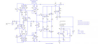
MOSFET output complementary IPS-VAS
Hi everyone,
I've simulated this circuit based on the circuit found on page 139, figure 7.10, of Designing Audio Power Amplifiers book by Bob Cordell, and it's an amplifier with complementary differential input stage with stabilized current mirrors, I wanted to know if this circuit will work in the real world?
I'm thinking about making a thermal shutdown circuitry connected to the Vmute network, using Schmitt trigger comparators and NTC voltage divider, I also wanted to incorporate a good S/C protection, but I don't know if I should use a single slope or multislope VI limiter. This circuit made by Bob Cordell seems very stable and with very good characteristics at the simulations. I had to use two 150pF capacitors instead of the 30pF ones to maintain a 45 degree phase margin, what is causing this effect?
MOSFET gate capacitance?
I also want to thank Bob for the Cordell Models, and for the LTSpice tutorial
Thank you very much for your attention,
Best regards,
Daniel Almeida
Attachments
Er.rrh! I'm really a speaker man. I would be very unhappy if you did this. Especially if I was an Electrostatic man.First get rid of the resistor in parallel with the output inductor; the resistor ruins the load isolation provided by the inductor.
With the greatest respect to Prof Cherry, his views of Thiele networks are obviously those of an amplifier man and don't take into account the evil things that us speaker designers like to do without restriction.See "Ironing out distortion" articles in EW by Cherry.
I had a similar argument with Peter Walker and Mike Albinson on the SOA protection on the 405. I like to think this had some influence on their later SOA networks.
If amp and speaker designers could agree to an impedance standard that would eliminate peaking, resonance, and conditional stability, while retaining complete modularity, then we would be set. Unfortunately ubiquitously present parasitics would limit the possible characteristic impedances to a range, and while this is necessary to stop parasitic mischief, it may be seen as overly limiting and inflexible. However without this, there is likely to be a degree of conditional stability in every setup.
To a passive component expert, amplifiers seem very mischievous. This is because passive components don't break into oscillation no matter what. But hooking up an amplifier to those passives can make damped circuits ring or oscillate. If the passives designer could treat an amplifier like a cable or wire with resistive or reactive loss, that would be one thing, but the amplifier can be a real wildcard.
I see two directions such a standard can take. The first is that the amplifier designer is constrained to make his amplifier to behave so that the load designer can treat it as a predictable passive component when connected to his network. The second is for the amp designer to be constrained to design the amp so that it is conditionally stable, but in a standardized way so that the skilled load designer can take advantage of the full damping factor of the amp. If the load designer doesn't want to, then it is simple to hook up the standard zobel network to revert to the former standard. The main purpose of the latter standard would be to reduce excess treble phase shift caused by impedance networks which become redundant for a skilled load designer.
One reason conditional stability persists may be that designers don't feel there is enough damping factor. The second standard would potentially remedy this situation.
- Home
- Amplifiers
- Solid State
- Bob Cordell's Power amplifier book