Frank,
Of course - you get one great big propagation delay (being a clock divider)") , but the edges are aligned up within say 5nS. The Audio data is shifted into the TAS5015 by the BCK from the SRC - so propagation delay between the Clocks is not an issue.
, but the edges are aligned up within say 5nS. The Audio data is shifted into the TAS5015 by the BCK from the SRC - so propagation delay between the Clocks is not an issue.
Yes, just connect the P661 directly to the TAS5015 HF-CLK.
John
Of course - you get one great big propagation delay (being a clock divider)
, but the edges are aligned up within say 5nS. The Audio data is shifted into the TAS5015 by the BCK from the SRC - so propagation delay between the Clocks is not an issue.Yes, just connect the P661 directly to the TAS5015 HF-CLK.
John
Hi,
a simple synchronuous frequency divider
Don't know anything about its jitter. But it is possible to extend easily.
Regards, Timo
a simple synchronuous frequency divider
Don't know anything about its jitter. But it is possible to extend easily.
Regards, Timo
Attachments
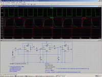
frequency divider
The edit button has gone...
Of course, R1, C1 & R2, C2 should be omitted in the real circuit, they should help to see the independence of the output from internal delays at the D-inputs for the simulation only.
On the other hand the small delays can make the decisions of the FFs more safe, because without them the preset time of the D-input is one propagation delay of the FF only.
In this case one must observe the maximum input transition timings to avoid oscillations or false triggering. Some months before I got this behaviour with a similar divide by two-circuit, driven by a µPower-comparator with transition times of 1µs, while the FFs were specified for max. 500ns clock input transitions. The use of Philips or TI parts with integrated Schmitt-Triggers helped.
It was a change to a second source whilst the running production.
Regards, Timo
Hi Pitch,
For lowest Phase Noise, I would combine L501 - L503 & R501 – R503, but still individually decouple each power pin (your 100n / 1n). By doing this, you will remove the potential (no pun intended) to having 3 different noise sources to the device. By combining the rails, any noise on the 3 power rails becomes common-mode internally to the P661, and the P661 is only degraded by ONE PSU noise source – and not the combination of 3.
What I mean to say is that if there were any noise difference between the power pins, this would be seen as an internal voltage difference – effecting internal logic transition points - thereby causing phase noise.
R512 should be reduced to around 27R (reducing resistor thermal noise).
John
Hi John and Frank,
I'm not familiar with such high quality clocks, let me ask you a question anyway.
I also would use only one PSU. If you use only one ferrite bead, but distant decoupling capacitors, you will possibly form a high-Q resonant circuit by the inductance of the traces and the capacitances. I believe, it could be better to use three independent decoupling circuits instead.
The resistor should be adjusted for optimal damping of the eventually resonances of the decoupling circuit (to preserve the low DC-impedance of the supply, the resistors may be transformed into parallel of the capacitors). I would do this by measuring the wanted signal, here the lowest jitter, if you got the possibilities to do this. It is not easy to determine the correct value of the damping resistor, it depends also on the impedance of the internal circuit behind the power pins.
Maybe, it seems to be a bit academic, but we talk about jitter in the ps range. One example: if one assumes a rise time of 1ns (linear edge) and a 3V supply (=3V gate output swing), then 3mV offset change at the internal comparator/gate inputs will cause 1ps deviation (seen as jitter). Who knows the PSRR of the internal comparator/gate circuits in the 1GHz-range (frequency according to 1ns rise time)?
Additionally, you will add the jitter of both VHC74s, using the asynchronuos divider.
The noise of the 47Ohm resistor is sqrt(4kTRB) =1.6 microV @ 1GHz, it will be reduced only by the sqare root of the value reduction, if I'm correct. This seems to be negligible.
A careful layout with matched impedances and length of the clock wiring is very important.
And I agree with John regarding the use of only one supply.
Again, I'm not an expert, maybe I'm fully wrong.
Best regards, Timo
The Phase noise introduced by the dividers is not important, as only jitter on the TAS5015 HF-clock is demodulated into the Audio Band (which is pre - dividers).
When I said “noise” of the series termination resistor, it’s not just a matter of simple “thermal noise” as I carelessly stated but: -
Higher impendence PCB tracking is more susceptible to noise pick-up , but more importantly drivers output impendence driving the clock line.
Due to the capacitive Miller effect seen on any MOSFET gate (CMOS logic), when input transverses the Logic state 0 to 1 or 1 to 0, a very high peak (say 70mA), but short (in the nS range) current is drawn by the CMOS input pin. This peak current is exactly at the Logic transition point, and if the driver has a high output impedance (or high value series termination resistor), the driver cannot instantaneously drive the Gate input pin though this transition point as it is current limited. The resultant delay causes a period of “logic level uncertainty” which results in phase noise, if the input is a clock.
I measured the current peaks with a small current probe designed for measuring LASER diodes, while only having a rated rise-time of 1.3nS, I still measured +/- 70mA 1.5nS peaks while drive the input of a single 74UHS04 gate!!! I would not like to hazard a guess of the real peak current (i.e. measured with a faster current probe).
So higher value series termination resistors increase phase noise not just because of their inherent thermal noise, but also because of the "current limiting" time delay they introduce during the logic level transition period.
As to the damping of the PSU, the most important point is to get the decoupling capacitors as close as possible to the power AND ground pins of the IC’s, then resistor damping of the PSU is largely irreverent – as we are only talking about a IC with a 5mm footprint! – a good PCB layout will have very short distances between power pins.
Cheers - John
Hi,
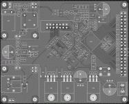
I have now almost finished my multiphase class D modulator board. It has optical SPDIF input, DIR1703 receiver, SRC4192 ASCR and TAS5076 modulator with all three input channels connected together. System clock is 24.576MHz. Since TAS5076 is I2C programmable , phase shift of outputs of can be adjusted on the fly, to experiment with different class BD modulation output stages.
The board is 80 x 100mm (exactly one half of Euro card) four layer design with top traces, GND, 3.3V and 5V layers. Input supply voltage is 12V and I have 3 fixed TO220 regulators for 8V, 5V and 3,3V. Digital decoupling is by generous use of 10uF, 6.3V X5R, 0805capacitors, I also use some Oscon and Panasonic SP caps. All decoupling caps have Murata BLM31B601S ferrite beads in their supply lines. Analog circuits have separate low noise power supplies consisting of dual NE5532 opamps (thanks-John).
Optical receiver and clock section are modular in design. There are piggyback connectors, so existing circuits can be substituted by 35mm x35mm piggyback modules. Optical receiver could be substituted for transformer isolated coaxial input or faster discrete design optical receiver.
Clock module can also be substituted, although it is even now quite flexible. There is place for both DIP8 can XO (Tentclock) and discrete Colpitts Jfet oscillator. Clock module is transformer coupled to the input of the AD8611 comparator, which then provides clock for the TAS5076, SRC4192 and DIR1703. I chose transformer coupling to prevent substrate injection currents into PLL circuit of the TAS5076.
I am unsure about some aspects of the design and and I seek some help.
1)DIR1703. As I understand, by using 24.576MHz clock, connecting CKSEL to UNLOCK and leaving BRSEL open, DIR1703 should lock onto any incoming SPDIF signal from32kHz to 96kHz. Can anyone verify this?
2)Split groundplane for PLLsection of TAS5076. PLL section contains AD8611 comparator and low noise power supplies for comparator and PLL part of TAS5976. Both groundplanes are connected with 1ohm resistor at the point where clock signal for SRC4192 and DIR1703 leaves PLLsection. Since TAS5076 evaluation module uses split ground plane i have provided one, but I am not sure if it is really necessary.
3) Clock circuit. I used JFET Colpitts oscillator that I have breadboarded and it gives nice sine wave about 1Vpp. There is also place for classic HC49/U can crystal and low profile HC49/4H can. Is there any difference between larger and smaller crystals regarding achievable jitter performance? There is also possibility to use 8.192MHz crystal and force it to oscillate at third overtone. Is there any advantage in using that approach?
Best regards,
Jaka Racman
Attachments
Hi Jaka,
Good to hear from you again, what a beautifully designed circuit diagram & PCB layout.
Every designer has his / her own design philosophy, so as you asked, I will add my own personal comments.
C101, C102, C103, C107, C108, C121, C122, C123, C125, C126, C137 & C138 should be bypassed with say 100N ceramic cap. The ESR of the 10uF will be to high – remember it’s the Rise & Fall time of the edges, translated in to frequency that determines to highest decoupling frequency required. Internally to the digital IC’s this can be say 100pS = 1GHz.
The oscillator circuit is too complex. I would loose the transformer AND the comparator. Despite what others may claim on this forum, comparators introduce significant phase noise, and should only be used in instances of very slow edges – but slow edges have no place in a low phase noise clock circuit. By far the best method to “Square” the edges is to use a high FT, High gain transistor.
Colpitts oscillators – especially ones using JFET’s, have MUCH higher LF (close-in) phase noise then the similar component count / cost - discrete transistor based Pierce XO. Pierce XO’s get bad press as they are normally configured around inverter gates. The transistor Pierce should not be tainted with the same brush.
FET based Colpitts XO do not perform well above say 10MHz. Above 10MHz; a bipolar transistor makes a better amplifier. The output resistance of a transistor emitter follower is 5 to 10 times lower then a JFET source follower, which allows the transistor to correctly drive the lower circuit impedance of a HF XO circuit. Also, the low crystal impedance at higher frequencies makes the medium input resistance of a transistor amplifier a better load for the crystal.
I notice that your using a FMMT618 as your XO Gain / Buffer stage, and I guess you selected it as larger transistors (high current types) have lower LF noise (due to there lower Rbb), but any benefit gain by using the 618 is total swamped by using the JFET, which produces massive amounts of LF noise (close-in carrier noise). Also, the Ft of the 618 is too low for fast output edges (especially at its low operating current in this application), slower edges result in higher phase noise – so again eliminating any befit gained from the 618 lower Rbb, use say BFS17 or better.
I would agree with you, and not break the ground plane around the clock circuit / PLL, this is only required when you have the potential for large PSU ground return currents flowing across / though the clock sections groundplane – which is not the case with your layout.
Isolated groundplanes increase the impedance between two points; allow HF potential differences between them - which will create phase noise if the clock line has to transverse these.
Also secondary MCLK frequency on the SRC should be offset from primary side MCLK – I would recommend 25MHz. SRC do not perform well with exact 1:1 input / output ratios.
Sorry, cannot comment on the DIR1703 or crystal “case size” phase noise performance – but DO ground the case of the crystal to a GOOD clean ground connection – otherwise the XO case will act as an antenna. Connecting to a poor ground point will do more harm then good.
John
DIR1703
Hi Jaca / John,
The DIR1703 is a very nice dig. receiver, although its datasheet is rubbish.
But connecting it like you did, supports 44.1 - 96 khz. So no problem there. I can tell from my own amplifier.
I'm in a hurry, so later more. Got to study your design later. Looks great @ 1st sight!!!
Cheers,
Frank
Hi John,
thank you for your comments. I will try to defend some of my choices, where I think they are right.
Decoupling caps: I use either ceramic 10uF 0805 caps or Panasonic SP caps. First ones have ESR less than 3mOhms and calculated ESL around 500pH. This 22uF Murata is even better. Second ones have ESR less than 12mOhms and ESL around 6nH. Typical 100nF 0805 X7R caps have ESR in tens of mOhms and ESL around 1nH. Where layout permitted I also used 100nF 0603 X2Y caps which have calculated ESL around 50pH. This may be an overkill because of the inductance of the chip leadframe. But I will add 10uF parallel to C103.
Comparator. I have chosen this particular type after I have read this post. Maxim Kochkurov characterized devices on Agilent phase noise measurement equipment with Rohde&Schwartz reference oscillator. Also from datasheet it seems that its output signal is relatively well behaved. I used comparator and transformer on the premise of split ground plane. If I loose split ground plane, then I would probably use BFT92 PNP differential pair as squaring circuit.
Colpitts oscillator. I have also breadboarded Pierce oscillator, but I used BFR92 (5Ghz ft) which was not optimal choice. Well sinewave had greater distortion than Colpitts and that was that. FMMT618 was used as an emitter follower and works quite well at 25MHz sinewave. I might try it as an oscillator, though I have read that PNPs are even quieter. This question is still open.
1 to 1 ratio on SRC. I think that 24.576Mhz clock on DIR1703 is used only to clock internal SPACT engine, and that output sampling rate of DIR1703 still follows input SPDIF frequency. Worst case input output ratio would be 1 to 4 (48Khz to 192Khz) or 1 to 2 (96kHz to 192Khz), but because SPDIF input does not track internal clock there will not be exact integer ratio. But I was considering option to add crystal to DIR1703 and that is still open since there is reserved place for this on the pcb. I will have to study what effect quality of SPACT clock has on DIR1703 output jitter.
I hope you will comment further.
Frank, thank you for encouragement regarding DIR1703. Hope to have your comment also.
Best regards,
Jaka Racman
BTW, if there is any interest I can make designfile available.
Hi Jaka,
Sorry, I didn’t notice that the 10uF where Ceramics and not electrolytics, but still feel uneasy where you have just an OSCON, such as in position C137 / C138 – the physical size of the OSCON prevents short track lengths, a 0603 can be adjacent to the IC pins.
Any chance on the data (or Web Link) on the 100nF 0603 X2Y caps you have used; I’m a bit out of touch with the latest capacitor footprints – I guess you used them in positions C145, C147 etc?
I’ve always used 0612 types for low inductance decoupling, but sounds like the 0603 X2Y are better?
I would leave the DIR1703 operating from the SRC 24MHz clock, having a second Async. clock frequency operating on the board is never a good idea.
Still stand by my comments on the JFET Colpitts, when you tried the Pierce you said you had a distorted waveform, but does distortion matter? Only M:S and rise / fall time (and phase noise, but you cannot normally tell from a waveform unless very poor).
I would still use a single transistor squaring circuit over a differential pair, as you only have the noise contribution of one device rather then the two in the differential pair – the lowest noise head-amps always use a single device input stage for this reason, luckily we don’t have to worry about distortion performance!
PNP are lower noise due to there lower Rbb, PNP’s normally have half the Base resistance compared to there NPN counterparts.
When characterizing comparators phase noise, there are many variables to consider, offset voltage, overdrive voltage, input edge speeds, operating frequency, common mode voltage, hysteresis etc… 1pS, but under which conditions? I know from experience that the AD8611 has poor LF noise performance (small input devices for speed?), but would you notice this when using the TAS PLL – I think not, the TAS PLL is going to be your designs limitation – but don’t under estimate the LF noise of a JFET XO circuit.
John
Hi Jaka,
Your observations on decoupling capacitors forced me into action, I finally download the Murata Chip S-Parameters and Impedance library – a major undertaking using my 28Kbps Internet connection…
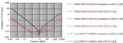
Interesting, for your information the Murata 0805 X5R 10uF 6.3V (Plots #2 & 3 on graph below), are better then your suggested Murata part 0805 X5R 22uF 6.3V (Plots #1 Blue & #2 Orange on graph) – and I guess cheaper.
But at the end of the day, good to see that the 0612 reverse format devices are still the best! (as I’m 2/3’s away though a large PCB design using them!) see Plots #5 Green & #6 Brown.
Checked out your lead on the X2Y caps, and seems that the 0612 is still better at high frequency for single rail PSU decoupling.
John
Your observations on decoupling capacitors forced me into action, I finally download the Murata Chip S-Parameters and Impedance library – a major undertaking using my 28Kbps Internet connection…
Interesting, for your information the Murata 0805 X5R 10uF 6.3V (Plots #2 & 3 on graph below), are better then your suggested Murata part 0805 X5R 22uF 6.3V (Plots #1 Blue & #2 Orange on graph) – and I guess cheaper.
But at the end of the day, good to see that the 0612 reverse format devices are still the best! (as I’m 2/3’s away though a large PCB design using them!) see Plots #5 Green & #6 Brown.
Checked out your lead on the X2Y caps, and seems that the 0612 is still better at high frequency for single rail PSU decoupling.
John
Attachments
Hi Jaka!
First of all, good luck with the amp!
I have used only the CS8416 192 kHz receiver. It has flexible configure methods, and many extras through I2C. If I were you, I use a discrete XO (like the "Tentclock in your schematics). Think about the noise added in the traces and the comparator will be a deal of phase jitter. The 100 ppm accurate clocks depend on their temperature, so it isn't phase jitter, it's only a deviance from the nominal frequency, (who would care about it if you have an SRC?) you shouldn't have an expensive 1 ppm accurate TCXO.
Gyula
Comments / questions
Hi
After a quite a look at your schematic the following:
Serial termination R 47 resp. 220R. Bit high in I2S lines?
Preferably use Coaxial instead of Toslink. Perhaps it is not immediately necessary to decouple input with transformer if the transmitter in your cd is coupled with a transformer. DIR1703 config looks good to me.
Why have you configured the input and output as slave of src and 5076 master? The way I see it is: SRC: input slave, out master@128 fs.
5076 slave. Or am I making a mistake here? Can you explain?
Nice to connect /RDY with MUTE on the SRC. Haven't thought of that.
And generally: can we make a statement about the best way to decouple: others need a long thread on this, but I think we can sort it out and than leave it. But I'm confused. For instance: what are those Reverse format devices. Is that a brand?
And where does that leave me with the ferrite bead, 1 u tantalum/100n ceramic combination?
Next, about clocks: 90% of this forum is filled with it. What's wrong with them chip clocks from let say: Phaselink: quite cheap and good perfomance. No comparator needed.
Happy designing all!
Hi,
Thanks for all the comments and best wishes.
John, you are right, I should parallel ceramics to the Oscons. But I think I have discovered another flaw in design. It is not good to supply both receiver and clock from same dual opamp, since HF noise on both outputs is not correlated.
Yes, 0612caps have lower (250pH) ESL, but they are not available in very high values. By paralleling 2 or 3 0805 hi capacitance caps similar ESL (380pH for 2, 240pH for 3) is achievable, but lower ESR. You also right about X2Y caps, they are mostly exotica, but in some places they fit nicely on PCB. Mainly I wanted to use caps that are easily available and Farnell stocks them all.
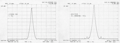
Regarding Colpitts, I have no other means of measurement but HP8568B spectrum analyser. I have compared my clock to HP internal reference oscillator and found no significant difference. See attached picture, left is reference oscillator, right is my clock. Frequency span is 1khz, at 100Hz offset noise is already 90dB down. This is does not imply that I am satisfied with the circuit, It is only first workable implementation. I will study oscillators some more, in particular some patents.
Regarding comparator, I think I will breadboard the circuit and see if there is anything worse on spectrum analyzer.
Gyula, I settled for DIR1703 since they claim excellent SPDIF jitter attenuation (75ps output jitter). I am also not quite satisfied with comparator choice, but it was also meant to be a squaring circuit for Colpitts and Maxim Kochkourov claims 1ps jitter for this device.
Frank, those 220R terminated lines were meant as limiting resistors for simple LED indicator, I2S lines are 47R series terminated. Perheaps 24R would be better solution, but that can easily be changed. I was mainly concerned about DIR1703 configuration, since it has such an excellent data sheet.
Re optical input. I know coaxial is better than Toslink. But my principal source will be PC which normally has optical digital output. Also someday I intend to use this modulator with very powerfull output stage, which will be very noisy in testing phase.
BTW, I intend to use new National LM5100drivers (HIP2100 compatible) and dual SO8 Siliconix Si7942DP fets in my proof of concept output stage.
Re TAS5076 master or slave, thanks for the warning, I will have to recheck my notes to see why I chose such configuration.
Re Phaselink, that would be my first choice, if they would be easily available. I could probably get samples through my job function, but I would prefer not to abuse that. Is there any online distributor ready to sell small quantity?
Re decoupling, I think there is a big difference in decoupling analog circuits (including DAC which are eminently analog circuits) and high speed digital devices running on 100Mhz clock. In latter case, ESL becomes the limiting factor and reverse format devices are nothing else than SMD ceramic capacitors with soldering pads along longer axis to decrease inductance. There was a nice thread showing effectiveness of large capacitance ceramic caps.
Best regards
Jaka Racman
Thanks for all the comments and best wishes.
John, you are right, I should parallel ceramics to the Oscons. But I think I have discovered another flaw in design. It is not good to supply both receiver and clock from same dual opamp, since HF noise on both outputs is not correlated.
Yes, 0612caps have lower (250pH) ESL, but they are not available in very high values. By paralleling 2 or 3 0805 hi capacitance caps similar ESL (380pH for 2, 240pH for 3) is achievable, but lower ESR. You also right about X2Y caps, they are mostly exotica, but in some places they fit nicely on PCB. Mainly I wanted to use caps that are easily available and Farnell stocks them all.
Regarding Colpitts, I have no other means of measurement but HP8568B spectrum analyser. I have compared my clock to HP internal reference oscillator and found no significant difference. See attached picture, left is reference oscillator, right is my clock. Frequency span is 1khz, at 100Hz offset noise is already 90dB down. This is does not imply that I am satisfied with the circuit, It is only first workable implementation. I will study oscillators some more, in particular some patents.
Regarding comparator, I think I will breadboard the circuit and see if there is anything worse on spectrum analyzer.
Gyula, I settled for DIR1703 since they claim excellent SPDIF jitter attenuation (75ps output jitter). I am also not quite satisfied with comparator choice, but it was also meant to be a squaring circuit for Colpitts and Maxim Kochkourov claims 1ps jitter for this device.
Frank, those 220R terminated lines were meant as limiting resistors for simple LED indicator, I2S lines are 47R series terminated. Perheaps 24R would be better solution, but that can easily be changed. I was mainly concerned about DIR1703 configuration, since it has such an excellent data sheet.
Re optical input. I know coaxial is better than Toslink. But my principal source will be PC which normally has optical digital output. Also someday I intend to use this modulator with very powerfull output stage, which will be very noisy in testing phase.
BTW, I intend to use new National LM5100drivers (HIP2100 compatible) and dual SO8 Siliconix Si7942DP fets in my proof of concept output stage.
Re TAS5076 master or slave, thanks for the warning, I will have to recheck my notes to see why I chose such configuration.
Re Phaselink, that would be my first choice, if they would be easily available. I could probably get samples through my job function, but I would prefer not to abuse that. Is there any online distributor ready to sell small quantity?
Re decoupling, I think there is a big difference in decoupling analog circuits (including DAC which are eminently analog circuits) and high speed digital devices running on 100Mhz clock. In latter case, ESL becomes the limiting factor and reverse format devices are nothing else than SMD ceramic capacitors with soldering pads along longer axis to decrease inductance. There was a nice thread showing effectiveness of large capacitance ceramic caps.
Best regards
Jaka Racman
Attachments
Hi Pitch,
Reverse format SMD devices have much lower impedance due to shorter physical distances between pads – combined with a larger contact area and lower resistance termination to the internal metalized layers.
E.g. 1206 has pads at opposite ends – and furthest apart, while the reverse format 1206, the 0612 has the pads on the closest parallel sides – which are also the widest.
The reverse format 0805 is 0508 etc.
The benefits of there lower impedance only becomes significant at above say 100MHz – but remember that the capacitor has to perform well at twice the operating frequency of the device, so if you have a logic Gate clocked at 100MHz, the PSU current is drawn at 200MHz (as you have 2 edge transitions per cycle).
When Jitter is no longer an issue (as we are using a SRC), I prefer optical transmission for the SPDIF. Not only is jitter a issue with SPDIF interconnect, but also coupling of RF noise – of which there is plenty inside your average poorly designed CD / DVD player. Optical interconnect removes the leakage current / RF issue - and the SRC the Jitter issues. Also, unlike electrical connections which can introduce large amounts of discrete 50Hz and 100Hz etc mains components due to chassis leakage current and earth loops, Optical transmission tends to introduce random phase noise – random is always preferable over discrete phase noise components – especially audio band spurie.
To get an idea of the leakage currents of typical CD / Transport units (!!! but do this only at your own risk !!!), just touch the Audio or Coax SPDIF outputs in one hand and touch a good earth point with the other hand – not a nice feeling! Just imaging how this mains leakage current is modulating our dearest ultra sensitive SPDIF data – and at low frequencies 50Hz etc, where the PLL clock recovery circuits in SPDIF receivers have ZERO attenuation!
To help meet EMC requirements, Transformer isolated SPDIF outputs are still AC coupled via a capacitor to the chassis of most CD / DVD players – the average SPDIF transformer also offers little HF RF isolation due to there inter-winding capacitance – I typically measure less then 10dB isolation at higher frequencies.
John
Reverse format SMD devices have much lower impedance due to shorter physical distances between pads – combined with a larger contact area and lower resistance termination to the internal metalized layers.
E.g. 1206 has pads at opposite ends – and furthest apart, while the reverse format 1206, the 0612 has the pads on the closest parallel sides – which are also the widest.
The reverse format 0805 is 0508 etc.
The benefits of there lower impedance only becomes significant at above say 100MHz – but remember that the capacitor has to perform well at twice the operating frequency of the device, so if you have a logic Gate clocked at 100MHz, the PSU current is drawn at 200MHz (as you have 2 edge transitions per cycle).
When Jitter is no longer an issue (as we are using a SRC), I prefer optical transmission for the SPDIF. Not only is jitter a issue with SPDIF interconnect, but also coupling of RF noise – of which there is plenty inside your average poorly designed CD / DVD player. Optical interconnect removes the leakage current / RF issue - and the SRC the Jitter issues. Also, unlike electrical connections which can introduce large amounts of discrete 50Hz and 100Hz etc mains components due to chassis leakage current and earth loops, Optical transmission tends to introduce random phase noise – random is always preferable over discrete phase noise components – especially audio band spurie.
To get an idea of the leakage currents of typical CD / Transport units (!!!
but do this only at your own risk !!!), just touch the Audio or Coax SPDIF outputs in one hand and touch a good earth point with the other hand – not a nice feeling! Just imaging how this mains leakage current is modulating our dearest ultra sensitive SPDIF data – and at low frequencies 50Hz etc, where the PLL clock recovery circuits in SPDIF receivers have ZERO attenuation!To help meet EMC requirements, Transformer isolated SPDIF outputs are still AC coupled via a capacitor to the chassis of most CD / DVD players – the average SPDIF transformer also offers little HF RF isolation due to there inter-winding capacitance – I typically measure less then 10dB isolation at higher frequencies.
John
Hi Jaka,
How did you download the screen-dumps from your HP8568B? If you ever need spares for your unit - I have a HP8568A RF section which I use as a spare source for my B's (same unit, just older uP).
Great Spectrum anaylsers - much better performance then the newer HP / Agilent designs!
I find the HP3585 (40MHz) better for low phase noise clock work, has greater dynamic range.
John
- Status
- This old topic is closed. If you want to reopen this topic, contact a moderator using the "Report Post" button.
- Home
- Amplifiers
- Class D
- Anyone interested in a digital amplifier project?