Yes Petter, you are right. The Kool Mu is available only in toroid and E shapes. I intended to use the E core because of the heat dissipation and the lack of money. The two core shapes with the biggest volume are written in the previos reply. I made the calculations for 25A RMS (35A peak) line current with 2mm wire diameter, the switching frequency is 200 kHz. In this range, the 26u material should be used to minimize the inductance fall caused by the core's flux density.
According to the calculations the toroid has 4.17W core and 34.375W wire power dissipation, and the inductance value is decreased to 45% of 400uH at the 35A peak line current. The core must be insulated from the winding layers, consequently the cooling is a little bit prevented, and the outer winding layers are also heating the core with 34W.
The E core has 4.76W core and 22.8W wire power dissipation, the inductance is decreased to 55% of 400uH at the peak line current. The E core has free areas for heat dissipating, but the wires are so close to each other, and instead of the toroid's 2 layers, here 4 layers of winding are required. At an extra plus, a shielding cover is also required around the core on the PCB, because of the firing flux.
So, this was my dilemma, and I don't think I made the right decision. This will be a resonant magnetic belch. It should be replaced..
  Does anybody need 26u Kool Mu E cores?
Petter, thank you for your hints!
Jaka wrote: "For your problem, I think the best solution would be to go back to the half bridge configuration, use as large MOSFETS as available and use such a small inductor to have circulating currents in 10-20A range. You will then have zero voltage switching most of the time, and if your FETS are large enough, parasitic diode will not even turn on if you have Rdson drop less than 0.5V."
I understood what were you hint at. You thought about the Class-D half-bridge. That might be working, and in that case the dead time can't be an effect of distorsion. But twice of the peak output current should be used for the coil dI. That is 42A at 96V for 4 Ohm. That willn't be done. I wrote about the Class-I half-bridge. But how can be the body diode turned on at positive Uds: "parasitic diode will not even turn on if you have Rdson drop less than 0.5V."? The pictures weren't accessible when I viewed the us20020053945 patent, I can't see the current transformer setup.
The APT's application note contains the series resonant ZVS topology. This topology assumes the series coil's current changes direction in every half-cycle. This is the precondition of the right polarity of self-induction voltage, and thus the ZVS. This case is assured only in the previous Class-D topology, when in a half-cycle the output coil's dI is greater than twice of the peak Iout.
Gyula
According to the calculations the toroid has 4.17W core and 34.375W wire power dissipation, and the inductance value is decreased to 45% of 400uH at the 35A peak line current. The core must be insulated from the winding layers, consequently the cooling is a little bit prevented, and the outer winding layers are also heating the core with 34W.
The E core has 4.76W core and 22.8W wire power dissipation, the inductance is decreased to 55% of 400uH at the peak line current. The E core has free areas for heat dissipating, but the wires are so close to each other, and instead of the toroid's 2 layers, here 4 layers of winding are required. At an extra plus, a shielding cover is also required around the core on the PCB, because of the firing flux.
So, this was my dilemma, and I don't think I made the right decision. This will be a resonant magnetic belch.
It should be replaced.. Does anybody need 26u Kool Mu E cores? Petter, thank you for your hints!
Jaka wrote: "For your problem, I think the best solution would be to go back to the half bridge configuration, use as large MOSFETS as available and use such a small inductor to have circulating currents in 10-20A range. You will then have zero voltage switching most of the time, and if your FETS are large enough, parasitic diode will not even turn on if you have Rdson drop less than 0.5V."
I understood what were you hint at. You thought about the Class-D half-bridge. That might be working, and in that case the dead time can't be an effect of distorsion. But twice of the peak output current should be used for the coil dI. That is 42A at 96V for 4 Ohm. That willn't be done. I wrote about the Class-I half-bridge. But how can be the body diode turned on at positive Uds: "parasitic diode will not even turn on if you have Rdson drop less than 0.5V."? The pictures weren't accessible when I viewed the us20020053945 patent, I can't see the current transformer setup.
The APT's application note contains the series resonant ZVS topology. This topology assumes the series coil's current changes direction in every half-cycle. This is the precondition of the right polarity of self-induction voltage, and thus the ZVS. This case is assured only in the previous Class-D topology, when in a half-cycle the output coil's dI is greater than twice of the peak Iout.
Gyula
Hi Gyula,
Here is the link which will now hopefully work.
I see you are still striving with class I. From your description I came to the conclusion that class I is maybe not the most suitable technology for open loop digital modulators, in spite that Crystal has been granted a patent on it. The patent has been granted, but there is still no chip to support it.
So I proposed you to go back to class D. When I said 10 to 20A , I also said ZVS most (not all) of the time. I hope you are not listening to the music with 3dB dynamic range") . I fear for your ears. I think it would be acceptable to depart from ZVS on music peaks only, and have lower losses when idling.
. I fear for your ears. I think it would be acceptable to depart from ZVS on music peaks only, and have lower losses when idling.
For your PFC project, I think 200kHz is to high. Keep it under 150khz and preferably even under 75kHz. Look at EMC requirements and you will see that they are a lot less stringent under 150kHz. Second , I suggest you build two phase shifted output stages. L4981 series chips from ST can be synchronised together. You can use smaller cores for that. In my PFC I use two 77439 cores with 39 turns single layer winding. And do not think that small gap in the core will produce fringing flux. 26ur material will have flux all over the place, even when using toroids. I know, I use it for resonant inductors.
Best regards,
Jaka Racman
Here is the link which will now hopefully work.
I see you are still striving with class I. From your description I came to the conclusion that class I is maybe not the most suitable technology for open loop digital modulators, in spite that Crystal has been granted a patent on it. The patent has been granted, but there is still no chip to support it.
So I proposed you to go back to class D. When I said 10 to 20A , I also said ZVS most (not all) of the time. I hope you are not listening to the music with 3dB dynamic range
. I fear for your ears. I think it would be acceptable to depart from ZVS on music peaks only, and have lower losses when idling. For your PFC project, I think 200kHz is to high. Keep it under 150khz and preferably even under 75kHz. Look at EMC requirements and you will see that they are a lot less stringent under 150kHz. Second , I suggest you build two phase shifted output stages. L4981 series chips from ST can be synchronised together. You can use smaller cores for that. In my PFC I use two 77439 cores with 39 turns single layer winding. And do not think that small gap in the core will produce fringing flux. 26ur material will have flux all over the place, even when using toroids. I know, I use it for resonant inductors.
Best regards,
Jaka Racman
Hi Jaka!
Don't take me serious all the time, I usually make some mistakes. I wrote a simulator program in C. Unzip the files to a free library if you want to try it. If it works (hope it will do something) the 6,7,8,9,u,i,h,j,b,n keys are usable to set some parameter: 6,7 : zoom; 8,9 : input signal frequency, 20 kHz originally, the step is 1 kHz; u,i : input signal amplitude, 90 V originally, the step is 5 V; h,j : the bca's two inductances' value, 22 uH originally, the step is 1 uH; b,n : the output capacitor's value, 350 nF originally, the step is 25 nF, t,z : load value, 4 Ohm originally, the step is 1 Ohm. The modulating signal's frequency is 384 kHz and the signal's amplitude is 50 V. Every signal has different colors: black grey is the modulating signal, silver grey is the input signal, yellow is the upper coil's voltage (+/-40 V), white is the lower coil's voltage (+/- 40V), green is the upper coil's current, cyan is the lower coil's current, red is the summed current from the two coils flowing to the capacitor and the output, blue is the output voltage. The load is 4 Ohm.
So, the essence is that the program gives different results for the inductors' curent as I wrote some reply ago. I don't know if the algorythm is bad or my idea was wrong. I thought the coils are conducting the output current alternately in the positive and negative output current cycles. I don't know which is true. According to the program's results the coils' current should just to be decreased to zero at the beginning of the next charging cycle, as you wrote.
About the MOSFETs' parasitic BJT I red it can be turned on only with fast positive voltage spikes between Drain and Source. In the 500 kHz SMPA article also appears the Uds shouldn't be higher that 0.5 V. This is nonsense.
For the PFC, I don't know the requirements. I have inquired about it in the post #355. I will investigate the L4981. It's already in my 1.2 Gigs literature. Till now I had my eyes on the UCC3818, and would like to syncronize with the UCC3895 for the output, and with a smaller converter for the digital and other parts. I planned to use with frequencies divided from the 24.576 MHz master clock. But it is near fixed to use 384 kHz for the SMPS stage because I could buy Ferroxcube TX63/38/27-3F3 toroids. 400 kHz is ideal for 3F3, and at this frequency 1.5 mm primary and 2*2mm (maybe square ) secondary winding can be done in 1 layer. That would disperse anything.. hehe I thought about the IRGP35B60PD for bridge switches, it has quite good body diode and low turn-off delay for 192 kHz.
I've seen the toroid. It has just 47.6 mm diameter, and 60u permeability. Hasn't it been sizzled in that 3kW PFC?
If I wereyou, I try the bca with the 6 phase modulator, it sounds so good, mostly at the highs. The class-d in my opinion is a worst choice for feedbackless modulators because of the deadtime.
Gyula
Don't take me serious all the time, I usually make some mistakes. I wrote a simulator program in C. Unzip the files to a free library if you want to try it. If it works (hope it will do something) the 6,7,8,9,u,i,h,j,b,n keys are usable to set some parameter: 6,7 : zoom; 8,9 : input signal frequency, 20 kHz originally, the step is 1 kHz; u,i : input signal amplitude, 90 V originally, the step is 5 V; h,j : the bca's two inductances' value, 22 uH originally, the step is 1 uH; b,n : the output capacitor's value, 350 nF originally, the step is 25 nF, t,z : load value, 4 Ohm originally, the step is 1 Ohm. The modulating signal's frequency is 384 kHz and the signal's amplitude is 50 V. Every signal has different colors: black grey is the modulating signal, silver grey is the input signal, yellow is the upper coil's voltage (+/-40 V), white is the lower coil's voltage (+/- 40V), green is the upper coil's current, cyan is the lower coil's current, red is the summed current from the two coils flowing to the capacitor and the output, blue is the output voltage. The load is 4 Ohm.
So, the essence is that the program gives different results for the inductors' curent as I wrote some reply ago. I don't know if the algorythm is bad or my idea was wrong. I thought the coils are conducting the output current alternately in the positive and negative output current cycles. I don't know which is true. According to the program's results the coils' current should just to be decreased to zero at the beginning of the next charging cycle, as you wrote.
About the MOSFETs' parasitic BJT I red it can be turned on only with fast positive voltage spikes between Drain and Source. In the 500 kHz SMPA article also appears the Uds shouldn't be higher that 0.5 V. This is nonsense.
For the PFC, I don't know the requirements. I have inquired about it in the post #355. I will investigate the L4981. It's already in my 1.2 Gigs literature
. Till now I had my eyes on the UCC3818, and would like to syncronize with the UCC3895 for the output, and with a smaller converter for the digital and other parts. I planned to use with frequencies divided from the 24.576 MHz master clock. But it is near fixed to use 384 kHz for the SMPS stage because I could buy Ferroxcube TX63/38/27-3F3 toroids. 400 kHz is ideal for 3F3, and at this frequency 1.5 mm primary and 2*2mm (maybe square ) secondary winding can be done in 1 layer. That would disperse anything.. hehe I thought about the IRGP35B60PD for bridge switches, it has quite good body diode and low turn-off delay for 192 kHz.I've seen the toroid. It has just 47.6 mm diameter, and 60u permeability. Hasn't it been sizzled in that 3kW PFC?
If I wereyou, I try the bca with the 6 phase modulator, it sounds so good, mostly at the highs. The class-d in my opinion is a worst choice for feedbackless modulators because of the deadtime.
Gyula
Attachments
Hi Jaka!
I added a feedback to the bca configured output in the simulation program, and the result is quiet good ! First I increased the two coils' leakage current to 256 mA/us, this was pretty dent the output signal. Second I added a +-10 V modulation voltage with frequency 3.4 * the input signal frequency and with 10 V amplitude of random noise to the 40 V supply voltage. After this I made a feedback to the input signal before the modulation by summing the input signal with twenty times the deviance (subtraction) of the normalized input and output voltage, and with a summed (integrated) error voltage. I found that the integrator is not necessary, only applicable with the subtractor, otherwise it cause ringing and excitation (slower integrator has no use). The integrating also caused a small phase shift, but the overall feedback caused a great phase correction in comparison with the input signal. The output signal is almost perfectly corrected after the feedback, and be independent from the coils' leakage and any torsition effects. I also tried the feedback with chopped input signal and the result was also very good. I think it is the effect of the subtractor, because it is always sense the actual deviance of the input and output, and is not slowed down by any operation. The response for the chopped signals (whose are containing high frequency components because of the chopping) seems to be depended only on the complex output filter's capability.
The attached file contains the modified program. If you want to see the results, unzip the files to a free directory! The signals and the keys are the same as I presented in the previous reply but the zoom was removed. The additional keys: 'o' : switches on/off the modulation of the supply voltage; 'p' : switches on/off the noise of the supply voltage; 'l' : switches on/off the input signal chopping; 't','u' : decrease/increase the load resistance, the original value is 4 Ohm, the minimum is 1 Ohm; 'f' : switches on/off the subtractor feedback, normally switched off; 'g' : switches on/off the integrator feedback, normally switched off; 'c','v' : decrease/increase the coils' leakage, normally 256 mA/us. The other modification keys are in the previous reply.
I suggest you first increase the input signal, switch the supply modulation and the noise on, leave the coils' leakage at the original value and see the output! Switch the chopping also on if you would like to.. Then decrease the input signal approximately by four and switch on the feedback! I'm going to make a low pass IIR or a fast integrator to smooth the output signal. Also would like to make a current feedback to see the results. I'm very curious.
The autotransformer patent link hasn't worked yet. The text is shown but the pictures are absent.
U.I.: Otherwise if you haven't got feedback in the bca, you should use it in 'Class-A'. Class-A means here to set the circulating currents' value half of the peak output current. The sound will be pretty good because the coils will not be exhausted during the operation, but the output signal will be modulated with the supply voltage. At the first run-up I would like to build a DSP founded bca configured amplifier with feedback, but neither of the modulators support input sample rates equal with the modulating frequency. Of course I think it will a base function some years later, when this architecture will be already used and spreaded by the amplifier giants...
Gyula
I added a feedback to the bca configured output in the simulation program, and the result is quiet good
! First I increased the two coils' leakage current to 256 mA/us, this was pretty dent the output signal. Second I added a +-10 V modulation voltage with frequency 3.4 * the input signal frequency and with 10 V amplitude of random noise to the 40 V supply voltage. After this I made a feedback to the input signal before the modulation by summing the input signal with twenty times the deviance (subtraction) of the normalized input and output voltage, and with a summed (integrated) error voltage. I found that the integrator is not necessary, only applicable with the subtractor, otherwise it cause ringing and excitation (slower integrator has no use). The integrating also caused a small phase shift, but the overall feedback caused a great phase correction in comparison with the input signal. The output signal is almost perfectly corrected after the feedback, and be independent from the coils' leakage and any torsition effects. I also tried the feedback with chopped input signal and the result was also very good. I think it is the effect of the subtractor, because it is always sense the actual deviance of the input and output, and is not slowed down by any operation. The response for the chopped signals (whose are containing high frequency components because of the chopping) seems to be depended only on the complex output filter's capability.The attached file contains the modified program. If you want to see the results, unzip the files to a free directory! The signals and the keys are the same as I presented in the previous reply but the zoom was removed. The additional keys: 'o' : switches on/off the modulation of the supply voltage; 'p' : switches on/off the noise of the supply voltage; 'l' : switches on/off the input signal chopping; 't','u' : decrease/increase the load resistance, the original value is 4 Ohm, the minimum is 1 Ohm; 'f' : switches on/off the subtractor feedback, normally switched off; 'g' : switches on/off the integrator feedback, normally switched off; 'c','v' : decrease/increase the coils' leakage, normally 256 mA/us. The other modification keys are in the previous reply.
I suggest you first increase the input signal, switch the supply modulation and the noise on, leave the coils' leakage at the original value and see the output! Switch the chopping also on if you would like to.. Then decrease the input signal approximately by four and switch on the feedback!
I'm going to make a low pass IIR or a fast integrator to smooth the output signal. Also would like to make a current feedback to see the results. I'm very curious.The autotransformer patent link hasn't worked yet. The text is shown but the pictures are absent.
U.I.: Otherwise if you haven't got feedback in the bca, you should use it in 'Class-A'. Class-A means here to set the circulating currents' value half of the peak output current. The sound will be pretty good because the coils will not be exhausted during the operation, but the output signal will be modulated with the supply voltage. At the first run-up I would like to build a DSP founded bca configured amplifier with feedback, but neither of the modulators support input sample rates equal with the modulating frequency. Of course I think it will a base function some years later, when this architecture will be already used and spreaded by the amplifier giants...
Gyula
Attachments
Hi Gyula,
you wrote a nice simulator. If you have not yet found out, here is the link to necesarry tiff plugin for browser. It seems that some sort of feedback will be necessary to get the ultimate performance from the digitaly modulated amplifier. But regretably all feedback schemes I saw to this day were more complicated than completely analog modulator.
Best regards,
Jaka Racman
As far as I know ICE don't sell their modules to individuals, but they may be obtained from LC Audio:
http://www.lcaudio.dk/com/index.php?page=7
I recon their prices are very reasonable.
Happy switching.
http://www.lcaudio.dk/com/index.php?page=7
I recon their prices are very reasonable.
Happy switching.
Hi Bolinder!
Thank you for the info! But pleaese don't estimate over our efforts!
Jaka! I think the output signal feedback isn't realizable with the TAS series of digital modulators because of the large processing delay. These modulators was originally constructed for simple audio applications, like television and other small power amplifiers with their TAS series output stages. I think the ultimate performace of TAS modulators can be reached with a direct connected headphone to their outputs.
I programmed a second-order Low-pass Butterworth IIR filter for the output in the simulation program. The output signal now can be evaluated better. The functions are the same as it was described in my previous reply and the filter can be switched on/off with the 'e' button. Unfortunately the filter causes additional phase shift. Maybe in the next version a linear phase FIR filter will be programmed.
Gyula
Attachments
Hi Gyula,
I was thinking about feedback around switching stage only taking PWM signal as a reference, not around modulator. Here are two links, first and second that will explain what was I thinking about.
I think John is also doing something similar, but with about an order of magnitude better results. I would be curious about his method once the intelectual property matters are settled. But until then, I also enjoy when he posts the results. It gives me a warm fuzzy feeling when I see what D class technology is capable of.
Best regards,
Jaka Racman
Hi Jaka!
This was my first thought too, but didn't know what is the information content of the separated integrated signal about the original signal in sight of distorsion and phase shift. So I didn't find any correct signal to compare the feedback with. Thank you for the link, I will take a closer look about them in a few days. At the first sight, the first is containing a PEDEC circuit.. Yes, it's that. It corrects only the duty-factor, but doesn't matter the output signal. I will post a few days later.
Gyula
This was my first thought too, but didn't know what is the information content of the separated integrated signal about the original signal in sight of distorsion and phase shift. So I didn't find any correct signal to compare the feedback with.
Thank you for the link, I will take a closer look about them in a few days. At the first sight, the first is containing a PEDEC circuit.. Yes, it's that. It corrects only the duty-factor, but doesn't matter the output signal. I will post a few days later.Gyula
Panasonic SA-Xr10
Does any one know if it is possible to set the xr10 to that it can play as a 'bi-amp' by using 4 of the amp's channels to drive two bi-wirable speakers? does this need programming on the chip? I tried using it in 'party' mode, but it did not soud right?!
What other mods have been tried on this amp?
Cheers
Peter
TAS3002 Help
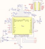
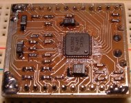
I have just finish building my second TAS3002 test board but it still isnt working!
I was wondering if someone could have a look and see what I am doing wrong. I have attached a Protel schematic+photo of a TAS3002 test board I have built.
However when I power up the board the 3.3V rail drops to 1.3V and the board sinks 450mA !!!
Help!
Mark.
Attachments
tas5012 vs tas5015
Hi
It is NOT easy to change from a TAS5012 to a TAS5015.
The TAS5012 uses an internal PLL to generate the 90MHz clock needed to do the PWM calculations.
The TAS5015 uses an EXTERNAL PLL - therefrore you can not easily change from TAS5012 to TAS5015.
Also the SA-XR10 layout and circuit design is optimized for the TAS5012 performance, and you will not gain by inserting the TAS5015 - the external circuitry and PCB layout is limiting the performance.
Seach this forum for SA-XR10 and you will find plenty of surgestions for improving the XR10.
rgds,
Kim
Hi Mark,
While I have no experience of the TI TAS3002, I had a quick look at your boards and schematic. At first glance, there appears not much wrong with the circuit, i.e. No outputs connected to GND / VDD, or reversed power connections.
The obvious aside, my attention would then focus on the PSU decoupling. If you take a closer look at the device decoupling, you will find extremely long & thin path lengths between the devices Vdd & Ground pins. It’s not helped by the fact that the AVdd & AVss are physically located on opposite sides of a QFPP! – A very bad device layout by Ti.
A 100n decoupling cap should be placed as close a possible to the package across pins 17 & 18, A ground plane under the IC from pins 3 & 4 (AVss) routed thou pins 36 & 34 (both NC), and a 100n decoupling cap from this ground plane to pin 35 (Avdd) – again directly on the PSU pins as close as possible to the package. Pin 18 DVss should also be connected to the ground plane under the device.
Remembering that you decoupling the internal die – DVdd to DVss & AVdd to AVss.
Best of luck,
John
TAS3002 board
Thanks for looking over the circuit and your comments. They are very valid comments and it was a tricky balance to get decoupling caps as close as possible to the pins and to also minimise/eliminate the need for vias as this is a homebrew pcb.
This dosn't however explain the reason for the significant voltage drop/current consuption of the IC. Its wierd that I made another board with this IC + the TAS5010 and although it did have another error, it exhibited a similar current consumption/voltage drop and it was configured significantly differently to this board.
I might have to resort to cutting tracks and measuring current consumption of various pins of the IC to track it down.
Any ideas anyone? Just after a little protoboard for this IC so I can play around with it!
- Status
- This old topic is closed. If you want to reopen this topic, contact a moderator using the "Report Post" button.
- Home
- Amplifiers
- Class D
- Anyone interested in a digital amplifier project?