cjd,
It looks like folks are happy with you reg. power supply layout as there have not been any comments for a few days.
I a not clear on the current status. Does the current layout implement actual part sizes?
If so and you think it is done (or at least can call it good for now) would you be so kind as to post a link to a pdf version of the artwork for the view (with parts) from the top view as well as etchable artwork as viewed from the copper side?
I've been digging up part specs and these are part of the result of that. In places where cap ranges are specified, you'll note I have allowed for three sizes to accomodate that. Where resistors are specified, I'm looking at a few seemingly common types people use and am trying to allow for all of those (within reason).
First up, half the power, use two for full setup. Mirror is do-able though I do sort-of question the value. The G/V markings are for the + side. I did spend just a little time so far working to get these combined on a single PCB with a combined ground at that point but it hasn't happened for me yet. I included an option to use a single huge cap though it goes off the board. Not sure if there's any value in this or not.

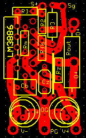
Next, LM3886 PCB for use with a regulated PS. A cap in the mute circuit would need to go under-board on this layout. Everything else could go up top if the mute resistor is the right type to fit between the chip pins. Ground connection is back to being jumpered so I could run traces to both V+ pins on the chip. Not sure why I missed that before.
The LM3875 PCB.

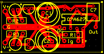
And finally, a go at a board for the OPA627 buffer, thanks to Carlos's schematic. This could be full of problems still.")
I'm working on a JFET buffer layout as well but have discovered some data sheets are missing information OR I'm missing knowledge to find the information on the data sheets. Probably the latter.
As normal, critiques are more than welcome.
C
First up, half the power, use two for full setup. Mirror is do-able though I do sort-of question the value. The G/V markings are for the + side. I did spend just a little time so far working to get these combined on a single PCB with a combined ground at that point but it hasn't happened for me yet. I included an option to use a single huge cap though it goes off the board. Not sure if there's any value in this or not.
Next, LM3886 PCB for use with a regulated PS. A cap in the mute circuit would need to go under-board on this layout. Everything else could go up top if the mute resistor is the right type to fit between the chip pins. Ground connection is back to being jumpered so I could run traces to both V+ pins on the chip. Not sure why I missed that before.
The LM3875 PCB.
And finally, a go at a board for the OPA627 buffer, thanks to Carlos's schematic. This could be full of problems still.
I'm working on a JFET buffer layout as well but have discovered some data sheets are missing information OR I'm missing knowledge to find the information on the data sheets. Probably the latter.
As normal, critiques are more than welcome.
C
One thing may be important (overlooked earlier... I am not into the non-inverted GCs). Feedback network, though it won’t carry currents higher than 1mA would be better connected to the central ground point independently of the signal ground. Might not be that hard to solve in the LM3886 case rotating R3.
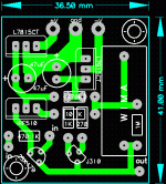
I am not sure if the path by which + reservoir cap is charged (currents may be as high as 10A) is too close to the regulator... Also, what is C3 on the reg board?
I am not sure if the path by which + reservoir cap is charged (currents may be as high as 10A) is too close to the regulator... Also, what is C3 on the reg board?
To make sure I understand:
R3 on the chip-amp boards should not go to signal ground but to power ground then? That may actually be easier on the 3875 board if it gets mounted behind the board. 3886 will probably require re-shuffling the components some again. Is a slightly long lead on one side OK here? (Preferable, I am sure, to a more convoluted output path)
C3 on the regulator board, I have no idea?! I'm going to go update that pic, so everyone else'll probably get all confused by your question. I know I had started playing with leaving room for small poly caps both from in+ to in- at the chip pins, and from V+ to G and V- to G, again at the chip pins. I'm assuming your comment on the + cap trace and regulator apply to this board? I'm not clear on this comment at all. As in physically too close? (should it just get moved up, or over some?)
r!sc! - that layout helps me a lot. Thanks!
And Pedja - inverted boards are in the works. They're required if these are to live up to my idea of being "stackable" to build paralleled and/or bridged setups, and I also know lots of folks still prefer that layout (especially with buffer, etc.)
C
R3 on the chip-amp boards should not go to signal ground but to power ground then? That may actually be easier on the 3875 board if it gets mounted behind the board.
3886 will probably require re-shuffling the components some again. Is a slightly long lead on one side OK here? (Preferable, I am sure, to a more convoluted output path)C3 on the regulator board, I have no idea?! I'm going to go update that pic, so everyone else'll probably get all confused by your question.
I know I had started playing with leaving room for small poly caps both from in+ to in- at the chip pins, and from V+ to G and V- to G, again at the chip pins. I'm assuming your comment on the + cap trace and regulator apply to this board? I'm not clear on this comment at all. As in physically too close? (should it just get moved up, or over some?)r!sc! - that layout helps me a lot.
Thanks!And Pedja - inverted boards are in the works. They're required if these are to live up to my idea of being "stackable" to build paralleled and/or bridged setups, and I also know lots of folks still prefer that layout (especially with buffer, etc.)
C
Let's say so.cjd said:R3 on the chip-amp boards should not go to signal ground but to power ground then?
But isn’t the Rfb already there? Also, I think a bit of care is needed as to where to put the pad for the resistor there, the chip leads will be quite close to the board. It may be good to put them in the line with the corresponding pins. Or anyway to make them just to be the pads, no holes.That may actually be easier on the 3875 board if it gets mounted behind the board.
I think it is more important to have a short feedback path than to save 2 or 3cm of the output path which is anyway long.3886 will probably require re-shuffling the components some again. Is a slightly long lead on one side OK here? (Preferable, I am sure, to a more convoluted output path)
I wouldn’t use a bypass PSU cap but would move electrolytics closer.
Yes, too close physically. I am saying what I see like a possible cause of the problems, I don’t know if it indeed will make problems or not. Maybe not. Maybe it will…I'm assuming your comment on the + cap trace and regulator apply to this board? I'm not clear on this comment at all.
Pedja
discreet reg
Pedja,
I built your ultimate reg. Made a few mistakes along the way (didn't fully discharge the caps before trying to resolder something, tested the validity of 2amp fuse by inadvertantly shorting the output, etc.). Anyway, got it together with 27 v zeners, 3055/2955 substituted for bd 912/911, and 150 ohms for R1 and R2. I get 24.1v output on the neg side and 24.4 on the pos side. On the pos side I get 850mv across R1, which means I could probably lower the value some. On the neg. side, I get no voltage across R2. Any ideas on what to check first? Replace the J309?
Somewhat related question; will the j309 substitute ok for the j310 in your buffer?
Thanks, I'm having fun with this,
Sheldon
Sheldon,Sheldon said:On the neg. side, I get no voltage across R2. Any ideas on what to check first? Replace the J309?
No voltage should appear across 1k gate resistor. Did you, by mistake, measure that one? Or none of these resistors show voltage drop and you have 0V measured directly between J309’s gate and source? If it is so, i.e. you have 0V there, check R2 itself (for short – you in fact can do this first of all).
Eventually you could report about the actual bias through that J309 if you connect some resistor of known value (something like 100R) in series with its drain.
Yes.Somewhat related question; will the j309 substitute ok for the j310 in your buffer?
Pedja
discreet reg
Ok, checked my circuit and found the error. Not surprisingly, it actually makes a difference whether or not the gate and drain connections are swapped. Anyway, I now get 5 volts across the 150 ohm resistor in the neg channel (33ma). Guess I fried the little ******. I'll try another j309.
Ok, checked my circuit and found the error. Not surprisingly, it actually makes a difference whether or not the gate and drain connections are swapped. Anyway, I now get 5 volts across the 150 ohm resistor in the neg channel (33ma). Guess I fried the little ******. I'll try another j309.
disreet reg
Didn't fry it after all. Just another wrong connection. All sorted now. I had the gate and source connections reversed, and one other wrong connection. I'm getting 5-6 ma current through R1 and R2 (measuring .85v across R1 and about .77v across R2). Is that ok, or should I drop the resistor values a bit? Otherwise good. I get +24.2 volts and -24.4. Now on to the buffer.
Thanks, by the way, for the very detailed notes and clear schematics. I'm at the very beginning stage of relearning some electronics. The theory takes a bit of work, but the hardest part is getting the practical tidbits. Yours are great.
Sheldon
warm up thump
Pedja,
Or anyone. If you are using the jfet buffer with a 1k resistor in the filter, couldn't you just short the buffer output after the resistor to ground during warm up? Or what value would be required to protect the buffer. Even if a relay were employed, it would be out of the circuit during run, so shouldn't hurt sonics?
Sheldon
A Newbie's Dumb Question
Forgive the novice's ignorance, but I am about to purchase a bunch of PCBs from BrianGT (LM3875TF) to construct some integrated Gainclone amps. Are these boards compatible with the ones that Brian is selling, and will these boards provide an active buffer stage suitable for use with the passive preamp (probably a DACT CT2-100K attenuator and Greyhill selector) I'll be installing along with Brian's PCBs in the chasses?
Forgive the novice's ignorance, but I am about to purchase a bunch of PCBs from BrianGT (LM3875TF) to construct some integrated Gainclone amps. Are these boards compatible with the ones that Brian is selling, and will these boards provide an active buffer stage suitable for use with the passive preamp (probably a DACT CT2-100K attenuator and Greyhill selector) I'll be installing along with Brian's PCBs in the chasses?
Re: A Newbie's Dumb Question
I think that the buffer should be able to handle any reasonable source, as that's it's function - provide a stable high input impedence for the source and a good low output impedence. But I have a very related and equally ignorant question. I'm also using Brians board and resistor values. I've built the buffer circuits and am now realizing major gaps in my knowledge of filters. Pedja, Brians board has a non-inverted input. It has a 220 ohm resistor in series with the input, followed by a 20k resistor to ground (I assume that the chip has a high input inpedence, so the impedence seen by the buffer would be 20k). How would you adjust your cap values (or do you?) to get the desired hf roll-off? Thanks for your patience with us beginners.
Sheldon
SRMcGee said:Forgive the novice's ignorance, but I am about to purchase a bunch of PCBs from BrianGT (LM3875TF) to construct some integrated Gainclone amps. Are these boards compatible with the ones that Brian is selling, and will these boards provide an active buffer stage suitable for use with the passive preamp (probably a DACT CT2-100K attenuator and Greyhill selector) I'll be installing along with Brian's PCBs in the chasses?
I think that the buffer should be able to handle any reasonable source, as that's it's function - provide a stable high input impedence for the source and a good low output impedence. But I have a very related and equally ignorant question. I'm also using Brians board and resistor values. I've built the buffer circuits and am now realizing major gaps in my knowledge of filters. Pedja, Brians board has a non-inverted input. It has a 220 ohm resistor in series with the input, followed by a 20k resistor to ground (I assume that the chip has a high input inpedence, so the impedence seen by the buffer would be 20k). How would you adjust your cap values (or do you?) to get the desired hf roll-off? Thanks for your patience with us beginners.
Sheldon
Sheldon,
With 22k the slope will go lower and roll-off at 20kHz will be about 0.2dB higher.
But you can always use 10k there instead, no?
If you stay at 22k you can use 910R instead of 1k to have about the same slope as with 1k-9k(or 10k) combination.
But again, I can not comment the filter’s consequences on the non-inverted GC, have not tried and a bit of experimenting won’t be bad anyway.
Pedja
Pedja said:Sheldon,
With 22k the slope will go lower and roll-off at 20kHz will be about 0.2dB higher.
But you can always use 10k there instead, no?
If you stay at 22k you can use 910R instead of 1k to have about the same slope as with 1k-9k(or 10k) combination.
But again, I can not comment the filter’s consequences on the non-inverted GC, have not tried and a bit of experimenting won’t be bad anyway.
Pedja
Thanks Pedja,
I guess the 20k shunt resistor value was originally selected to work with a pot directly tied to the front end of the amp, and acts as a voltage divider with the pot to set input sensitivity and impedence, which changes with pot position? With the buffer, it makes sense that I can change that value to anyting that the buffer itself can drive. I think I''m gradually getting it. I'll see what resistors I've got on hand. Almost there. I'd like to fire this thing up today.
Sheldon
Re: warm up thump and grounding question
Ok, now I'm going to prove that a little knowledge can be dangerous. I've got some extra j309's. How about drain to buffer output, source to ground and gate to a cap and resistor to ground, powered by =15 volts from the buffer reg.? If I understand correctly (a very dubious assumption), output from the buffer should flow to ground until voltage on the gate comes up enough to shut it off. Time would depend on the cap and resistor values. Any chance?
On the grounds- I finished the buffers. I left the 20k shunt resistor and used two 15nf polystyrene caps in parallel for C2 and a 4.7nf polystyrene cap for C1, separated by a 914R. I have a ground wire that connects the ground terminals of the buffer regs. I have attached the caps to that ground and had planned to connect that, in turn, to the signal ground on the chip (Brian GT's non-inverted clone). I was also going to connect the buffer input ground to the same wire. Bad idea? Should I use a separate ground for the regs and signal paths? Or are the reg. grounds low enough current to not interfer with signal?
Great thread, by the way. Lots of good info from everyone. Hope I'm not taking it too off track.
Sheldon
Sheldon said:Pedja,
Or anyone. If you are using the jfet buffer with a 1k resistor in the filter, couldn't you just short the buffer output after the resistor to ground during warm up? Or what value would be required to protect the buffer. Even if a relay were employed, it would be out of the circuit during run, so shouldn't hurt sonics?
Sheldon
Pedja said:Yes, it can be done that way.
Ok, now I'm going to prove that a little knowledge can be dangerous. I've got some extra j309's. How about drain to buffer output, source to ground and gate to a cap and resistor to ground, powered by =15 volts from the buffer reg.? If I understand correctly (a very dubious assumption), output from the buffer should flow to ground until voltage on the gate comes up enough to shut it off. Time would depend on the cap and resistor values. Any chance?
On the grounds- I finished the buffers. I left the 20k shunt resistor and used two 15nf polystyrene caps in parallel for C2 and a 4.7nf polystyrene cap for C1, separated by a 914R. I have a ground wire that connects the ground terminals of the buffer regs. I have attached the caps to that ground and had planned to connect that, in turn, to the signal ground on the chip (Brian GT's non-inverted clone). I was also going to connect the buffer input ground to the same wire. Bad idea? Should I use a separate ground for the regs and signal paths? Or are the reg. grounds low enough current to not interfer with signal?
Great thread, by the way. Lots of good info from everyone. Hope I'm not taking it too off track.
Sheldon
Can of worms
Hi All-
I know I am opening a can of worms here but I have to ask the question. Please excuse me if it has been asked before.
I have been using the Marchand XM-1 crossovers for years with no issues. Since they have a unity gain from in to out, couldn't they also be used as a buffer for the gainclones?
Of course they would also introduce a filter but if you were using a sat/sub system that would be a good thing.
So would the XM-1 make for a decent buffer or is the circuit design too dated?
Thanks, Troy
- Status
- This old topic is closed. If you want to reopen this topic, contact a moderator using the "Report Post" button.
- Home
- Amplifiers
- Chip Amps
- Any interest in GC input buffer and power supply regulator pcb's?