Any better? should still be room to use a trimpot vs. resistor if someone wanted to do that I think - or, the layout could be shortened up a bit. I addressed all the items Pedja brought up as best I understand them, which very well may mean I still missed something. ") This layout doesn't lend itself to a mirror image that I've been happy with, but that's probably not troublesome at all.
This layout doesn't lend itself to a mirror image that I've been happy with, but that's probably not troublesome at all.
It's just half again of course since it'd just be a copy/paste to get the other half, and that's a bigger pic. Why put you all through that bandwidth crunch?
C
This layout doesn't lend itself to a mirror image that I've been happy with, but that's probably not troublesome at all. It's just half again of course since it'd just be a copy/paste to get the other half, and that's a bigger pic. Why put you all through that bandwidth crunch?
C
I've switched to a top view since that's probably what I should have been using from the start anyhow...
Slightly revised, with a mirror image that I think may be adequate. Not really sure. Anything that I'm doing that isn't really quite right let me know (really wrong, I'd hope you mention) The one on the right is the same as previously posted (with some small changes to the traces only). The left is a new layout.
I've started looking at the buffer, as well as looking at the basic chip-amp circuit layout, so we'll see if I get anywhere that I'm happy with.
Thanks to all that have commented so far.
C
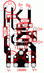
All this got me to thinking about a minimized PCB for the chip-amp portion since you don't need big caps any more... I came up with this.
Single sided board (though the R from pin3 to pin8 should really be mounted right to the pins, there's room for it). There is room for a zobel, for those that might want it also. There is one jumper here, but it connects power ground to signal ground, where I believe its normal drawbacks may actually be an advantage... I think.
So, as usual, the question is... any good?
I wasn't sure about putting the output ground separated by O+ so far, but that keeps the ground traces shorter overall and that seemed to be the more sensible approach...
Still working on a buffer idea. I just got inspired as to the solution for this while toiling on the buffer. Odd how something just in your peripheral vision and working in the back of your mind, suddenly solves itself. I hope.
C
Single sided board (though the R from pin3 to pin8 should really be mounted right to the pins, there's room for it). There is room for a zobel, for those that might want it also. There is one jumper here, but it connects power ground to signal ground, where I believe its normal drawbacks may actually be an advantage... I think.
So, as usual, the question is... any good?
I wasn't sure about putting the output ground separated by O+ so far, but that keeps the ground traces shorter overall and that seemed to be the more sensible approach...
Still working on a buffer idea.
I just got inspired as to the solution for this while toiling on the buffer. Odd how something just in your peripheral vision and working in the back of your mind, suddenly solves itself. I hope. C
Yes it is pretty nice.
Maybe that V- line could be routed left of (behind) the chip, so Rfb can go beneath the board and between two rows of chip’s pins?
It is not a long shared path but it might be not that hard to connect the Zobel to the PSU caps ground point independently of the signal ground. Speaker ground should be taken from the same PSU caps central point.
I just like the rest.
Pedja
Parallel LM3886 board?
Hi C-
Since you are learning and tuning your skills, would you like to make a parallel LM3886 board?
I need one for a project, and my drawings have not been coming out as neat as yours.
The schematic is attached.
Thanks in advance,
Troy
Hi C-
Since you are learning and tuning your skills, would you like to make a parallel LM3886 board?
I need one for a project, and my drawings have not been coming out as neat as yours.
The schematic is attached.
Thanks in advance,
Troy
Attachments
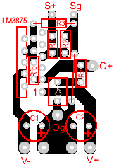
oook. round two. I didn't mention previously but this is for the LM3875. I'll peek at the 3886 here in a bit.
The output ground is where you suggested I put it Pedja - that doesn't keep the connections quite as clean as I might like but I think it's in a spot such that it's not a problem, and hopefully the better placement as far as components goes will outweigh any other concerns.
Depending on the type of resistor you use, Rfb can probably go topside under the chip pins. If you're using premium components, I suspect you may also just choose to solder direct to the chip pins for that one.
Parallel layout, eh? And of the 3886? One thing at a time! And really, I should probably build something one of these days. I did get some parts today finally!  but not for a regulated PS - just a normal NIGC for now.
I just noticed, I don't have any place to bypass the caps with a small poly... should there be here? Also, the power cap spots should probably be set up to accept a small range in sizes since tuning those seems to be suggested by some.
Pedja - is the discrete regulator enough better that it would make more sense than the LM338 board? I mean, with a PCB most of the misery is gone, right?
C
round two. I didn't mention previously but this is for the LM3875. I'll peek at the 3886 here in a bit.The output ground is where you suggested I put it Pedja - that doesn't keep the connections quite as clean as I might like but I think it's in a spot such that it's not a problem, and hopefully the better placement as far as components goes will outweigh any other concerns.
Depending on the type of resistor you use, Rfb can probably go topside under the chip pins. If you're using premium components, I suspect you may also just choose to solder direct to the chip pins for that one.
Parallel layout, eh? And of the 3886? One thing at a time!
And really, I should probably build something one of these days. I did get some parts today finally! but not for a regulated PS - just a normal NIGC for now.I just noticed, I don't have any place to bypass the caps with a small poly... should there be here? Also, the power cap spots should probably be set up to accept a small range in sizes since tuning those seems to be suggested by some.
Pedja - is the discrete regulator enough better that it would make more sense than the LM338 board? I mean, with a PCB most of the misery is gone, right?
C
here's a shot at the 3886 without implementation of the mute. I didn't dig too far yet to see if pin 7 always goes to ground but it was a straight shot so it's there right now. More reading of spec sheets will come. edit: I still didn't read anything on this, so that leads me to believe it should be connected.
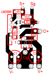
One additional question: Would it be better to have separate traces for all the power ground points all come together at a single central point to the large mass to which they're all connected right now?
C
edit: I still didn't read anything on this, so that leads me to believe it should be connected.
One additional question: Would it be better to have separate traces for all the power ground points all come together at a single central point to the large mass to which they're all connected right now?
C
Parallel LM3886 board time line
Hi C-
Wow... When I said a LM3886 board, I meant at your leisure... Please don't kill your self because of my request!!
I simply asked because your work was coming along well, and you appeared to be enjoying it.. I certainly don't want you to become burned out on it..
Please ignore my request until a time you have "spare" time to practice.
I think the regulator board was coming along fine and I am looking forward to the buffer portion as well.
Please excuse my suggestion of the 3886 until/if YOU are ready.
Thanks again, Troy
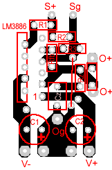
For the LM3886, I think this slight tweak will allow parallel circuits with as many as you choose. I believe you'll want to leave R2 off the boards and use just one at input (?) - same with the cap at input for parallel circuits. Output can come straight off the pin or through a resistor hence the dual O+ options. I have seen some suggestions that this R be used on a single board anyhow. I'm not sure whether trying to put two chips on a single board for a parallel circuit outweighs the potential to just stack as many single chip boards as you want/need.
I moved Rfb back outside the pins of the chip in case pin7 should go to the power ground directly not signal ground. If not it leaves some room to open up the schematic and insert the mute circuitry...
As for time, trust that you aren't causing me to miss anything at all. My mother in law is in town (out shopping with my wife) and it's pouring rain down.
I think I need to work on a better bypassing scheme... any suggestions would be helpful.
C
I moved Rfb back outside the pins of the chip in case pin7 should go to the power ground directly not signal ground.
If not it leaves some room to open up the schematic and insert the mute circuitry...As for time, trust that you aren't causing me to miss anything at all. My mother in law is in town (out shopping with my wife) and it's pouring rain down.
I think I need to work on a better bypassing scheme... any suggestions would be helpful.
C
C,
Yes, it seems it widened somehow… No need to move PSU caps to make a space for the speaker ground, just take that from the caps central point and make a track of few cm so you can make another pad. Bypass caps can be mounted beneath the board, though with 100u or smaller caps necessity for them becomes lesser.
I think the layout is generally very good and I think it is now most important to determine the definitive size of the parts.
Yes, the discrete (non-f/b) reg is IMO better. I have, however, two reasons not to deal with it at the moment. The first is that we may get better if doing one thing at the time, and the second is that after some late cases here I am reluctant to do some things publicly.
Pedja
GC input buffer
I apologize to all those who have contributed to development of the GC buffer for my mention of lm3886 taking us "off track". Pedja is right. We are better when we do just one thing at a time. I also wish I could do something for Pedja's concern #2. Thank You Pedja, however I'm afraid my gratitude won't alleviate issues brought on by others.
Sincerely,
Request to move to a new thread.
Hello Moderators-
May I ask you to move the following posts to a new thread in the Chip Amp forum in a title similar to "Parallel LM3886 amp"? They seem to hijacked this thread, and for this I apologize.
1. http://www.diyaudio.com/forums/showthread.php?postid=429419#post429419
2. http://www.diyaudio.com/forums/showthread.php?postid=429434#post429434
3. http://www.diyaudio.com/forums/showthread.php?postid=429900#post429900
4. http://www.diyaudio.com/forums/showthread.php?postid=429932#post429932
5. http://www.diyaudio.com/forums/showthread.php?postid=429975#post429975
6. http://www.diyaudio.com/forums/showthread.php?postid=431424#post431424
edit: Include this post to please!
Thank you in advance,
Troy
Please move this one too
Hi, I was too quick in my reply to the HiJacked post of CJD as he already mentioned the track possibility in his text.
Now i studied the PCB and text better I see taht the space can be used for the additional PosPower pin No.5. Although fron the NS data sheet you could read that it is not abolutly required, it is always the best to use all available Power pins.
More serious might be that the mute resistor is not on the PCB, This is in fact an unmute resistor and without it there will be no music from the chip.
Use 39k and it will supply the min 0.5 mA from a power supply of 22 V DC upwards. The capacitor is for delay but also decoupling. Probably 10 uF or more is OK when no delay is required, else 100uF or more might be OK.
Rick
Attachments
I personally do not have a problem with LM3886 here, it is in fact about a few needed changes… Its mute pin, as Nick just noted, can be used for power up delay, this spells LM3886 gives the possibility to deal with the buffer’s power up thump by one capacitor.
Though paralleled chips would probably lead us a bit further from where we are now.
Pedja
Though paralleled chips would probably lead us a bit further from where we are now.
Pedja
Too late to edit... Sorry, I've meant Rick.Pedja said:(...) as Nick just noted (...)
I've stepped back a bit and am researching parts (to get exact sizes!) In doing this, my lack of experience in this field is becoming rather obvious - I don't know which versions of what to use! So some help here would really be appreciated, and I can keep chugging along on doing these PCB's. Things have been through a couple revisions already (on the chip boards anyhow) since I've posted previously, but I'm waiting to post again till I have part sizes down better.
I've also dug up a couple programs for designing these.
One question I have is this: Should I stick single sided? There are some advantages both ways, but I suspect double-sided wouldn't be something you could go etch yourself? But if it turns into some kind of group-buy, I think things start to get vaguely reasonable at 50 boards for manufactured, double sided with solder masks and silk-screen.
And, I actually don't feel the chip boards are out of place here, since going regulated in particular means much smaller caps at the chip. So it's a package thing in my mind. I'm looking at ways of putting this all on a single PCB so that it can be left as one piece or broken up. I'm also trying to make the amp boards in such a way that you could turn them "sideways" and run solid core wire through a stack of them to parallel them. I haven't looked at inverted topology yet to see about bridging possibilities.
C
cjd said:
One question I have is this: Should I stick single sided?
I guess I would vote for single sided if the layout experts end up happy with the layout from a performance point of view.
My thinking is that folks could try the design sooner as they could more etch it themselves rather than have to wait for a possibly one time group buy. In addition having a version that folks could easily etch allows a lot more flexibility for integrating for example the power supply into an existing gainclone.
If the true target was a group buy though, there is no doubt that professionally manufactured double sided boards are a beautiful thing.
- Status
- This old topic is closed. If you want to reopen this topic, contact a moderator using the "Report Post" button.
- Home
- Amplifiers
- Chip Amps
- Any interest in GC input buffer and power supply regulator pcb's?