Which is where you can actually get a 4PDT relay for the speaker - that will actually BREAK the circuit instead of welding together in the event of a fault. Without spending $80 on it. DC protect problem solved.
Yep! But I haven't been in Orlando for some time now and it will be some time before I get back there.
I do like the SSRs with those new mosfets though. This is nice and much faster than the relays, plus we can easily command them and put them in more places.
I see one on each rail, plus at least one on the output. This might even be good enough to forgo the use of the limiters. And perhaps instead of limiting, the sensing done for limiting could be used in some other way to trigger those other protections.
We're all always thinking about the low distortion, squeezing whatever we can from the amp, and then we continue using those limiters, which if properly calculated can work effectively while making their presence as scarce as possible, but when driving an amp hard, we're bound to have them make some impression, and there goes the low distortion...
I'm seriously thinking about doing away with the limiters, if the switches can really do the job and prevent the damage.
If you're worried about the .05% distortion that rectification in the contacts causes, you're building the wrong amplifier")
Not so much, but I think the impact of the limiters can be probably more than what's caused in the switches, whether relays or especially mostfets.
I have a fairly large stash - enough for the next 20 or so builds. Most of them came from Skycraft, as well as half the heat sink inventory. Who do you think bought out all their good stuff 10 or so years ago? They haven't had as much since.....
Cool! I haven't been there in over 5 years, I don't even know how they're doing now. I wish other such shops were more widely available. I don't know of anything even close anywhere near, or far, from where I am at the moment. Pitty! I would like to poke around their heatsinks right now.
Personally, I would not forego the VI limiters in favor of tripping a relay. A relay is probably fast enough, but it does interrupt the music. If it happens because the speaker wires get shorted, it's ok. If it happens during a party, I'd rather listen to a bit of distortion than have the music(?) completely interrupted for a couple seconds. That might start a riot. Or get some smartawq saying your amp is a piece of
I'm sure the VI limiters will add measurable distortion when not activated but driving a 2 ohm load. At 4 ohms with only 1/2 the current you'd never even know they're there.
I'm sure the VI limiters will add measurable distortion when not activated but driving a 2 ohm load. At 4 ohms with only 1/2 the current you'd never even know they're there.
Personally, I would not forego the VI limiters in favor of tripping a relay. A relay is probably fast enough, but it does interrupt the music. If it happens because the speaker wires get shorted, it's ok. If it happens during a party, I'd rather listen to a bit of distortion than have the music(?) completely interrupted for a couple seconds. That might start a riot. Or get some smartawq saying your amp is a piece of
I agree, and Michael Kiwanuka even mentioned, I think in post #20 of that thread about his paper, that the SSR relays could be tripped to remove power from the amp in case of soa violation. That is definitely not something I would consider. I'd rather use that signal to trigger compression at the input for example.
The show must go on, so I wouldn't be in favor of anything that interrupts it when it's not a matter of survival (of the speakers and amp).
I'm sure the VI limiters will add measurable distortion when not activated but driving a 2 ohm load. At 4 ohms with only 1/2 the current you'd never even know they're there.
My thinking about this, is that since I never myself make any use of any amp under a 4 ohms load, I would design the amp for 4 ohms, with the protections tuned to be above that and have enough headroom in the outputs to handle any worst such case (reactive and all), but then I would only use the amp with 8ohms and the protections would never even come close to be activated. How about that? I'm even sometimes thinking about having 16ohms speakers, but I would not consider series or paralleling any speakers. They would have to be 8ohms or 16, whatever, but not 4. I think 2ohms is riddiculous, and when designing a bridge, then we can think of aiming for 4 ohms, which is normal, since we can load it with 8 and each sides sees 4.
I'm not yet fully versed in the grounded bridge, but this is a very interesting topo, because we can actually bridge a bridge...
Well, I've been trying to work out the calculation in a spreadsheet, based on Michael's fine paper, and I just can't fall back on the same results as he does. Before I can calculate new values, I want to make sure I make the proper calculations by re-doing his and trying to find the same results, but this isn't working so far.
I'm trying with fig.28, and following the steps, which refer to fig.29-30-31-32, but I'm not even going any further than fig.29/30 for now, because my results are not right.
First I tried solving in reverse the equation (8), using the values found and injecting them back into the equation, but it doesn't match. I find a result of 0.74566 instead of the 0.6. That's a big difference and perhaps he made some serious adjustments when choosing the actual values.
Then it gets worse with the next ones.
Looking at the next equation with the 0.6/R2. First I don't see where that 3.72 is coming from, then same thing with the 4 in the (4-3.72) part. And finally, as I look at the following step where the substitution is done, I don't understand how the - got there after R1, because as I understand the maths (limited), to me (4-3.72) is positive, so I fail to see where that - comes from.
What I do find for the current and voltage for R3, is that since we are assuming having the 40V from the output transistor's emitter, and we have 37V52 on the other side of R3 (fig.29), that's 2V48 on R3 and 24.8mA passing through. This seems correct to me. But then trying to figure out R1 gets tricky...
Spookydd,
Equation 8 computes correctly viz 3.08*22.7/(22.7+1500*100/(1500+100)) =
0.600395 (R1 should be 1536.36 for greater accuracy)
At point A on Fig 27 : Ic=14A, Vce=0 thus from Fig29:
Vout = 40V – 0.22*14A = 36.92
Vbase = 36.92+0.6 =37.52V
VRe = 0.22*14A = 3.08V
Because Vce = 0V, R1 and R3 are effectively in parallel and 3.08V appears across (R1//R3) + R2.
Thus 0.6/R2 = 3.08/(R2+R1*100/(R1+100))...
At point B on Fig27: Ic=4A, Vce=36V thus from Fig 30: ReR3 node = Vcc-Vce = 40-36 = 4V
Vout = 4V – 0.22*4 = 3.12V
Vbase = 3.12+0.6 = 3.72V....
Thus R1 and R2 can be established
Here you are correct. That’s a misprint. Eqn 9 should read 0.6 = R2(36.28/R1 + 0.28/100) That’s something I’ve often meant to point out to Mike, but never did. It seemed fairly obvious.
I hope this helps clear up any confusion. I think it really is a quite elegant solution Mike has offered.
I’ve attached a pdf of my spreadsheet showing Mike’s design example, corroborating the calculated values he’s established.
Brian
Attachments
Equation 8 computes correctly viz 3.08*22.7/(22.7+1500*100/(1500+100)) =
0.600395 (R1 should be 1536.36 for greater accuracy)
Ok, obviously it's my lack of mastery of the basic math mechanics. I was grouping with parenthesis to preserve the order but I messed that up. So in the spreadsheet I had to remove 3 sets of parenthesis that I had wrongly added
. Drats! poor math skills!At point A on Fig 27 : Ic=14A, Vce=0 thus from Fig29:
Vout = 40V – 0.22*14A = 36.92
Vbase = 36.92+0.6 =37.52V
VRe = 0.22*14A = 3.08V
Because Vce = 0V, R1 and R3 are effectively in parallel and 3.08V appears across (R1//R3) + R2.
That much I had figured, if I hadn't screwed up the calculations with improper use of parenthesis.
I was basically stuck at the point, which wasn't very far, just because I couldn't verify my calculations being correct.
It's good to put this into a spreadsheet, make sure it works, then never make the same mistakes again.
At point B on Fig27: Ic=4A, Vce=36V thus from Fig 30: ReR3 node = Vcc-Vce = 40-36 = 4V
Vout = 4V – 0.22*4 = 3.12V
Vbase = 3.12+0.6 = 3.72V....
I got lost there because I didn't make the switch to the other assumptions for the point B. I was mistakenly staying with the point A! Duh!
Here you are correct. That’s a misprint. Eqn 9 should read 0.6 = R2(36.28/R1 + 0.28/100) That’s something I’ve often meant to point out to Mike, but never did. It seemed fairly obvious.
Ouch!
No wonder it got even more confused! It seemed obvious to me the sign was incorrect, however I'm not confident enough with the math mechanics to be certain.I hope this helps clear up any confusion. I think it really is a quite elegant solution Mike has offered.
This should be much better now, with your skillful explanations. Mike has done a great job explaining everything. It's not him, it's me not being up to the task to fully grasp the process
.I hope I can continue with this later in understanding how to properly calculate the topo used by leach.
I’ve attached a pdf of my spreadsheet showing Mike’s design example, corroborating the calculated values he’s established.
Very nice of you to help so much. Thanks a bunch!
It will take me some time to digest everything, and I will verify and re-verify before going further. I want to get this right and make a spreadsheet that works. (and the amp)
There is one point that I wanted to address though: As AndrewT mentioned before, the protection transistors do start to turn on way before the 0.6V that we use for threashold, and this changes everything. We definitely don't want to "hear" that protection when it comes to act, and making calculations with a hard threashold at 0.6V seems to me like it's not going to give us the "non-interference" we're looking for.
This main issue is that this makes the protection action far too progressive and it starts acting a little bit far earlier than we calculate.
If we took a much lower Vbe threashold value in the calculations, then the 0.6 or 0.7V point would be likely to be well above the soa and that would defeat the whole purpose and make a protection that doesn't work right.
How are we supposed to handle this?
Use .6 volts, and set the trip point to about 25A, which is above the normal current. Remember, the transistor Ic/vbe is exponential, NOT linear. It won't trip at .5 volts. Not enough to matter anyway.
Alright, I will do what I can and make several plots with different values so I can compare.
I have lots of info now to dig into and digest. It will take some time to go through it all and have enough understanding of it. I will continue building that spreadsheet and post it so everything can be re-checked after me.
I am also pondering about using SSRs, as they can really bring extra safety and they're really not that expensive to implement. If we want a reliable and safe amp, this may be an option to make use of.
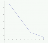
Here is a plot of the the 2N3055 SOA that I managed to make. This is not a hyperbolic curve, it's based only on the datasheet and I plotted it using the points at the knees for the DC curve on the datasheet SOA.
It seems to me that the simple dual slope locus with its knee (point B) somewhere not far from the secondary breakdown knee on the SOA graph should work very well. Plus looking at the available SOA "above" that, and having 3 pairs outputs, even 25A seems very conservative and as long as the protection prevents leaving the SOA, we can allow for more current. The 25A split into 3 pairs is below 8.5A and we have so much left over headroom above that, we could bring this up some more.
The AB slope could be steeper.
There is one detail that comes up however. Michael mentions that the slope with the segment BD must intersect the Vce axis higher than the rails if we want to insure against spurious action. However this is a problem, because we already have the rails a little above the breakdown max voltage, which is already outside the SOA at that spot, so by pushing the intersection of the locus even further above that, we're not making a safe locus.
This is what we get for pushing the limits on those trannies beyond the recommended. What should we do about that?
One thing that might be a good idea when picking the actual transistors, beyond the matching, is to test their secondary breakdown. Apparently it's quite common for those types to have that secondary breakdown higher than the stated one on datasheets, and it's probably why there are so many amps built with the rails so much higher than permitted. So a little extra testing to make sure they can handle it is a good thing to do.
We're not looking to get 100V like on those 3055H, but 70 or 75, maybe even 80V is probably possible.
Attachments
Testing for secondary breakdown turn over point is probably destructive testing.
i.e. you have the find the lower breakdown current, when Vce is higher than the turnover Vce.
This implies that you have identified that too much current has been drawn.
And how do you keep the Tj=25°C, during the test?
i.e. you have the find the lower breakdown current, when Vce is higher than the turnover Vce.
This implies that you have identified that too much current has been drawn.
And how do you keep the Tj=25°C, during the test?
Testing for secondary breakdown turn over point is probably destructive testing.
i.e. you have the find the lower breakdown current, when Vce is higher than the turnover Vce.
This implies that you have identified that too much current has been drawn.
And how do you keep the Tj=25°C, during the test?
For one thing, the transistor under test would have to be on a big enough heatsink just like it should be under real use.
I've seen some tests of the breakdown done before, and many manufacturers screen their parts for just that as well. So it's done all the time. So there must be a non-destructive method to do it. I think a current limiting to a very low value and proceeding "very" carefully is part of the solution.
I don't have a ready method at the moment, but since I know it's being done a lot, there has to be a way.
This would ensure the transistors chosen will survive the excess by design that we are imposing on them.
While I was searching for a 2N3055H datasheet that would show the 100V Vce0 and the SOA chart for it, I compared the various sheets and there is one parameter that I'm wondering about:
There is on the ST datasheet an indication of a VceR which is slightly higher than the Vce0 and it would be with a RBE <=100ohms. They don't explain or show some test schematic for that and there is no note about that RBE.
I'm taking this as using the transistor with a base resistor up to 100ohms, and this would allow a slightly higher Vce0 sustainable. Is this right?
We can't use such a high value in the base, as I feel the drivers would have to work too hard to be able to push the outputs all the way, especially since we're having 3 pairs. We have a 10ohms right now in the bases, which is more or less similar to other topos out there. Would that 10ohms in the output's bases allow us a tad of extra headroom on that Vce0???
We're pushing our luck a bit by aiming for 35V rails, and I am planning to use a 2x24V transformer, on which I measured an unloaded output at 26.9V lately. This was probably with 235V more or less on the primary, which is very common where I am. I'm sure once hooked up and a little bit of idle current is drawn, with the various drops, in the rectifier bridge and other places, I should have unloaded rails probably in the 35-36V range, and they would sag a little with increasing load.
It would be really good to be able to screen the 2N3055s for their Vce0 (non destructively). I've seen patent filings dating back to the late 60s for such non-destructive test aparatus for just that. So it's been around for a long time and obviously used by many amp manufacturers and the likes.
I don't have this handy, but I remember in the past having looked at a tester that could check that Vce0 safely. Someone must know of this and perhaps could propose something useful. I'm sure many would be interested.
Testing for s/b limits can be made non-destructive, but it's a fairly involved setup. What you have to do is apply Vce at Ic (in a pulsed mode), and monitor Vbe. The insatnt Vbe drops (indicating thermal run away), shut it down in a couple microseconds. Testing to see if a device passes a DC spec is easy. Just set the device up as a current source at the VCE you're testing - with a big emittter resistor and 15V or so at the base. Large emitter resistor makes for a stable Ic. Mount the device on a finned heat sink and put the fins in an ice bath.
You really don't need to go to this much trouble for 3055's. If you use ST's, ON (Motorola), NOS GE/RCA (newer epitaxial), NOS Siliconix, or any other major maker from the 80's on, they'll work. I would screen for VCEO, but that's just a matter of having a high voltage supply and a 10K high watt resistor on hand. Heat it up with a soldering iron until you can't touch it and monitor where breakdown is. ST's will be about 100V, ON's will be about 200 (yes, 200). Just size you resistor so that you'll only get about 5mA at the lowest expected Vceo and you can't hurt anything. If you get a bunch that take over 100V that you want to use, you can also apply 100V through a lower resistor value and re-screen for Iceo the take the best ones.
I had a bunch of no-mane 3055's that were sitting in a drawer for years till I built my last 3055 amp. I had marked them with a sharpie with the Vceo and Vbe values so matching was easy when I got around to using them.
Testing for s/b limits can be made non-destructive
That's what I thought and since there are old patents out there about doing just that, it can be done.
, but it's a fairly involved setup.
So perhaps there is a device to make for this (start a new thread???), and more could use this to screen their parts.
What you have to do is apply Vce at Ic (in a pulsed mode), and monitor Vbe. The insatnt Vbe drops (indicating thermal run away), shut it down in a couple microseconds. Testing to see if a device passes a DC spec is easy. Just set the device up as a current source at the VCE you're testing - with a big emittter resistor and 15V or so at the base. Large emitter resistor makes for a stable Ic. Mount the device on a finned heat sink and put the fins in an ice bath.
Can we doctor up some little tester apparatus for this? In a new thread, we can discuss a design, and I wouldn't mind doing a pcb layout for it.
I had this in mind before, mostly for matching the parts, but we can do this for the Vce0 test as well.
You really don't need to go to this much trouble for 3055's. If you use ST's, ON (Motorola), NOS GE/RCA (newer epitaxial), NOS Siliconix, or any other major maker from the 80's on, they'll work.
...
ST's will be about 100V, ON's will be about 200 (yes, 200).
Are you serious?!?! They "advertise" the original data, more or less, in their current datasheets, so I suppose we can't count on it, and it's definitely not guaranteed. Bu this is good to know.
I had a bunch of no-mane 3055's that were sitting in a drawer for years till I built my last 3055 amp. I had marked them with a sharpie with the Vceo and Vbe values so matching was easy when I got around to using them.
Mine are old stock, some from the 70s and most from the 80s, so I won't count on better manufacturing and better performances, but still, even back then, many old parts sometimes had higher Vce0 possible than stated in the datasheets.
I think this is worth testing for and making sure, since we're pushing our luck with a design that's a bit over the allowed limit in the first place, it would be stupid to just make a bet.
By the way, does my SOA graph for the 2N3055 look ok?QUOTE]
I don't think so.
Attachments
Ok, I see now why I was wrong about the SOA charts. I'll be working on this over the weekend.
But in the mean time, while digging into some old info, I found an old interesting one, 2N3055/MJ2955 based, but quite unusual.
It's from an old elektor, but the concept apparently came from a japanese guy who found this was a way to have a class A amp without the dissipation issues. And apparently he made a 350W class A amp that way. (not this one of course)
Curiously, not only it is made with 2 amps, but it also does some type of funky flying rails, mixed with a class A amp half and the other half is class B. Weird ain't it? But this should work.
This one is only a 15W, but it's using the 3055/2955!
Attachments
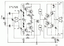
This one is only a 15W, but it's using the 3055/2955!
For a 15 watt amplifier, I would use TIP41/42 output devices....
"This one is only a 15W, but it's using the 3055/2955! "
Lots of room for improvement there. I would sneek in some bias on the slave amp, perhaps making it a CFP with a gain of 3x, and run it on ±30V. You could get 50W out of it (if desired).
Yamaha made an amplifier with this topology a while back.
Lots of room for improvement there. I would sneek in some bias on the slave amp, perhaps making it a CFP with a gain of 3x, and run it on ±30V. You could get 50W out of it (if desired).
Yamaha made an amplifier with this topology a while back.
- Home
- Amplifiers
- Solid State
- Amplifier based on 2N3055