Various
Hello Edmond
Very nice work on the output stage.
The KSC2690 and KSA1220 used in the output stage design as pre drivers and for the biasing network my question is if a part with greater current capacity were to be used to beef up the pre drivers does this mean the same part in the bias network must also be upgraded.
By the way how are you finding Micro-Cap 10 it get the impression the simulators convergence has improved is this right.
Regards
Arthur
>>I'm sure you have already checked it as a part of your design work, but I would like to hear how bias circuit behave when the amplifier clip?
Best regards,
Mogens
Hello Mogens
If you build an amp with quite a few output devices and high enough supply rails I think you can easily build a amplifier that will not clip before your domestic speakers distort.
Regards
Arthur
bias
Thank you !
They don't need to be the same. The only requirements for the bias trannies are that they are medium sized (say Ic max. cont. = 1A) to get (about) the right TC and a convenient package to mount them on the heat-sink or on top of the OP devices without to much thermal losses.
I haven't installed V10 yet, so I can't say nothing about it.
In the meantime I got a working bias version with the TT-diodes, based on the same concept as Vbe multiplier version. But I'm not really happy with it, as it is rather complex:
six extra trannies plus sixteen R's, two caps and a trim pot.
So what to do? Just skip the idea of a universal bias circuit (i.e. a PCB that can be used with bias trannies as well as TT-diodes)? Perhaps it is too ambitious and/or needless complicated (unless I got the right inspiration, from stinius perhaps )
)
Cheers,
E.
Hi Arthur,Hello Edmond
Very nice work on the output stage.
Thank you !
The KSC2690 and KSA1220 used in the output stage design as pre drivers and for the biasing network my question is if a part with greater current capacity were to be used to beef up the pre drivers does this mean the same part in the bias network must also be upgraded.
They don't need to be the same. The only requirements for the bias trannies are that they are medium sized (say Ic max. cont. = 1A) to get (about) the right TC and a convenient package to mount them on the heat-sink or on top of the OP devices without to much thermal losses.
By the way how are you finding Micro-Cap 10 it get the impression the simulators convergence has improved is this right.
Regards
Arthur
I haven't installed V10 yet, so I can't say nothing about it.
In the meantime I got a working bias version with the TT-diodes, based on the same concept as Vbe multiplier version. But I'm not really happy with it, as it is rather complex:
six extra trannies plus sixteen R's, two caps and a trim pot.
So what to do? Just skip the idea of a universal bias circuit (i.e. a PCB that can be used with bias trannies as well as TT-diodes)? Perhaps it is too ambitious and/or needless complicated (unless I got the right inspiration, from stinius perhaps
)Cheers,
E.
PCB
Hello Edmond
>>So what to do? Just skip the idea of a universal bias circuit (i.e. a PCB that can be used with bias trannies as well as TT-diodes)? Perhaps it is too ambitious and/or needless complicated (unless I got the right inspiration, from stinius perhaps )
I think that if it is possible to do two separate designs one for each output device type because I think you are right its a needless complication to a PCB.
So I propose we go to completion with the Sanken output devices as the direction we should take at this stage, what do you think.
Regards
Arthur
YGM
Cheers
stinius
Hi Stein,
I got the mail and schematics. Thank you so much.
Cheers,
E.
Hello Edmond
>>So what to do? Just skip the idea of a universal bias circuit (i.e. a PCB that can be used with bias trannies as well as TT-diodes)? Perhaps it is too ambitious and/or needless complicated (unless I got the right inspiration, from stinius perhaps )
I think that if it is possible to do two separate designs one for each output device type because I think you are right its a needless complication to a PCB.
So I propose we go to completion with the Sanken output devices as the direction we should take at this stage, what do you think.
Regards
Arthur
Hi Arthur,
I also think it's better to not merge the two versions into a single PCB. It's too complicated and causes too much delay.
Another possibility: what about splitting the PCB in two parts: one for the front-end (IPS and VAS) and one for the OPS. Then we only have to change the latter for a TT version and keep the front-end PCB unchanged.
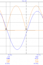
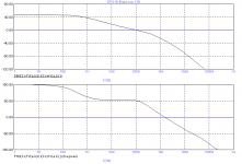
In the meantime I have modified the OPS a bit. Now the bias peaking at Vcc=5V has gone (see 2nd pic). Also the cross-conduction at 200kHz is lower and symmetrical (see 3rd pic). Both are about 260mA at the positive-going transition, respectively negative-going transition, instead of 530mA and 345mA (as in post 60). Notice the different base stoppers.
Cheers,
E.
PS: More details to come: the common mode and differential loops.
Attachments
Bias circuit (continued)
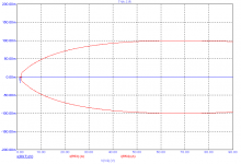
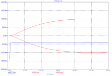
Opposed to the majority of bias circuits, this one works differently. Actually in the same way as Bob Cordell's cq. Malcolm Hawksford's error correction OPS: Instead of adjusting the bias voltage at the inputs of the (pre-) drivers by means of a temperature dependent voltage source, this one senses the base to base voltage of the OP transistors by means of a temperature dependent current source (Q17 & Q18), which output is fed back to I-V stages (Q15 respectively Q16), which in turn add a voltage between the pre-drivers and main drivers. As with any FB system, also in this case we must pay attention to the loop properties. Without frequencies compensation it appears that the phase margin is way too low. So I added C24, C25, R42 & R43 (btw, just a simple Miller compensation). Now the loop is stable, see 1st. pic. DC gain = 53dB, PM = 91 deg @ 100kHz, GM = 23dB @ 860Hz.
It should be noticed that this kind of bias circuit isn't disturbed by Vbe variations of the (pre) drivers. So no need to put them on the same heat sink and/or add another compensating thingy that monitors the temperature of them separately.
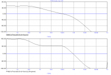
We are still not done, as there is one more FB loop. By means R38 and R40 it is ensured that the voltages across Q15 and Q16 are equalized. Without this provision one of them will saturate. See the next pic for the gain and phase response. DC gain = 46dB, PM = 91 deg @ 1.4kHz, GM = ~32dB @ ~ 38MHz. Given these figures, no need for further frequency compensation.
One more remark: the current through Q17 & Q18 is not fixed, rather it varies with the supply voltage. This would result in a variable bias. However, R45 & R46 compensate for this unwanted side effect, at least for supply voltages of interest (see 2nd pic of the previous post).
Cheers,
E.
Opposed to the majority of bias circuits, this one works differently. Actually in the same way as Bob Cordell's cq. Malcolm Hawksford's error correction OPS: Instead of adjusting the bias voltage at the inputs of the (pre-) drivers by means of a temperature dependent voltage source, this one senses the base to base voltage of the OP transistors by means of a temperature dependent current source (Q17 & Q18), which output is fed back to I-V stages (Q15 respectively Q16), which in turn add a voltage between the pre-drivers and main drivers. As with any FB system, also in this case we must pay attention to the loop properties. Without frequencies compensation it appears that the phase margin is way too low. So I added C24, C25, R42 & R43 (btw, just a simple Miller compensation). Now the loop is stable, see 1st. pic. DC gain = 53dB, PM = 91 deg @ 100kHz, GM = 23dB @ 860Hz.
It should be noticed that this kind of bias circuit isn't disturbed by Vbe variations of the (pre) drivers. So no need to put them on the same heat sink and/or add another compensating thingy that monitors the temperature of them separately.
We are still not done, as there is one more FB loop. By means R38 and R40 it is ensured that the voltages across Q15 and Q16 are equalized. Without this provision one of them will saturate. See the next pic for the gain and phase response. DC gain = 46dB, PM = 91 deg @ 1.4kHz, GM = ~32dB @ ~ 38MHz. Given these figures, no need for further frequency compensation.
One more remark: the current through Q17 & Q18 is not fixed, rather it varies with the supply voltage. This would result in a variable bias. However, R45 & R46 compensate for this unwanted side effect, at least for supply voltages of interest (see 2nd pic of the previous post).
Cheers,
E.
Attachments
2 pcb
Hello Edmond
>>Another possibility: what about splitting the PCB in two parts: one for the front-end (IPS and VAS) and one for the OPS. Then we only have to change the latter for a TT version and keep the front-end PCB unchanged.
I think making the amplifier on 2PCBs is a good idea.
Regards
Arthur
Hello Edmond
>>Another possibility: what about splitting the PCB in two parts: one for the front-end (IPS and VAS) and one for the OPS. Then we only have to change the latter for a TT version and keep the front-end PCB unchanged.
I think making the amplifier on 2PCBs is a good idea.
Regards
Arthur
The Mongrel lives on.I think making the amplifier on 2PCBs is a good idea.
Eureka?
Hi guys,
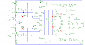
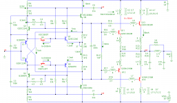
As I was still obsessed by the idea of a 'universal' bias scheme, I did some more work. I seems that I finally got the right right inspiration. By changing the polarity of the bias control transistors (Q3...Q6), I could omit two of the six extra trannies and some Rs. Now the TT version needs 'only' four of them. BTW, just as many as a lot of other symmetrical designs. Regarding the 'BJT bias controlled' version, just replace the TT-diodes, by suitable diode-connected BJTs, adjust some resistor values and omit P2 in series with the 'left over' TT-diodes. That's all.
Below the TT-version, BJT-version and startup behavior of the TT-version. More graphs in the next post.
The blue trannies should be reasonably matched* (PNP to PNP, respectively NPN to NPN) and kept at the same temperature (i.e. Tamb).
Notice that spice models are not always that accurate. So be prepared that in real life some resistor values need to be adapted.
Also notice that the 'left over' diodes (D3 & D4) have another function: namely to diminish the cross-conduction under severe test conditions.
Cheers,
E.
PS: cc3 = 18nF and rc3=100R
edit: * from the same lot.
Hi Arthur,
[snip]
In the meantime I got a working bias version with the TT-diodes, based on the same concept as Vbe multiplier version. But I'm not really happy with it, as it is rather complex:
six extra trannies plus sixteen R's, two caps and a trim pot.
So what to do? Just skip the idea of an universal bias circuit (i.e. a PCB that can be used with bias trannies as well as TT-diodes)? Perhaps it is too ambitious and/or needless complicated
Hi guys,
As I was still obsessed by the idea of a 'universal' bias scheme, I did some more work. I seems that I finally got the right right inspiration. By changing the polarity of the bias control transistors (Q3...Q6), I could omit two of the six extra trannies and some Rs. Now the TT version needs 'only' four of them. BTW, just as many as a lot of other symmetrical designs. Regarding the 'BJT bias controlled' version, just replace the TT-diodes, by suitable diode-connected BJTs, adjust some resistor values and omit P2 in series with the 'left over' TT-diodes. That's all.
Below the TT-version, BJT-version and startup behavior of the TT-version. More graphs in the next post.
The blue trannies should be reasonably matched* (PNP to PNP, respectively NPN to NPN) and kept at the same temperature (i.e. Tamb).
Notice that spice models are not always that accurate. So be prepared that in real life some resistor values need to be adapted.
Also notice that the 'left over' diodes (D3 & D4) have another function: namely to diminish the cross-conduction under severe test conditions.
Cheers,
E.
PS: cc3 = 18nF and rc3=100R
edit: * from the same lot.
Attachments
Last edited:
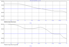
And here's the response of the common mode (=bias) loop, differential loop (that equalizes Vce of Q3 & Q4) and the startup properties of the BJT controlled version.
edit: The electrical overcompensation, intended to compensate for thermal resistances, is about 30 to 40%.
Cheers,
E.
edit: The electrical overcompensation, intended to compensate for thermal resistances, is about 30 to 40%.
Cheers,
E.
Attachments
Last edited:
Hi Edmond,
This is a really nice circuit you have come up with. I'm sorry I haven't had more time to look at this. I'm tempted to breadboard the Sanken circuit, to check the temperature stability.
And the front-end is still the one a few pages back?
Btw. Christmas holiday on friday ;-)
Best regards,
Mogens
This is a really nice circuit you have come up with. I'm sorry I haven't had more time to look at this. I'm tempted to breadboard the Sanken circuit, to check the temperature stability.
And the front-end is still the one a few pages back?
Btw. Christmas holiday on friday ;-)
Best regards,
Mogens
Hi Mogens,
In principle, the front-end is still the same. But, as with any change, I have to simulate all loops all over again (a lot of work!), in particular the clamping loops. Probably some changes will be needed.
@ Arthur & Mogens,
Thank you!
Cheers,
E.
edit: I just discovered an error in the 2nd schematic on post 73. Wrong O/P devices! Must be Sankens. Sorry.
Last edited:
Errata
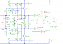
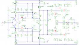
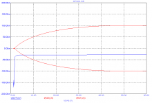
Here's the correct schematic for the Sanken devices. Notice that also P1 and R13 have been modified (now they are the same as in the TT version).
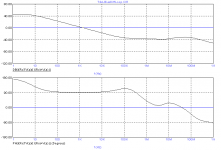
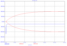
The electrical overcompensation is 50:39, by which I mean that if the O/P device are 50 degrees above ambient temperature, you will get the same bias (100mA) if the temp. sense trannies (Q5 & Q6) are 39 degrees above Tamb, see 2nd pic.
Sorry for the confusion (probably due to my 'Iron Condors', who also need some attention).
Cheers,
E.
Here's the correct schematic for the Sanken devices. Notice that also P1 and R13 have been modified (now they are the same as in the TT version).
The electrical overcompensation is 50:39, by which I mean that if the O/P device are 50 degrees above ambient temperature, you will get the same bias (100mA) if the temp. sense trannies (Q5 & Q6) are 39 degrees above Tamb, see 2nd pic.
Sorry for the confusion (probably due to my 'Iron Condors', who also need some attention).
Cheers,
E.
Attachments
Hi Edmond, I like a lot the symmetry of this circuit, care to summarize the advantages over a standard bias circuit that would justify the extra complexity? How can this circuit extended to more than two output pairs?
Why is the 330nF cap between the bases still required? I thought you can avoid it in this kind of setup?
The 22uF caps are a PITA. Are they really required to be so large (I would think not) and is there any way to avoid them at all?
Why is the 330nF cap between the bases still required? I thought you can avoid it in this kind of setup?
The 22uF caps are a PITA. Are they really required to be so large (I would think not) and is there any way to avoid them at all?
Hi Edmond, I like a lot the symmetry of this circuit, care to summarize the advantages over a standard bias circuit that would justify the extra complexity? How can this circuit extended to more than two output pairs?
Why is the 330nF cap between the bases still required? I thought you can avoid it in this kind of setup?
The 22uF caps are a PITA. Are they really required to be so large (I would think not) and is there any way to avoid them at all?
Hi YWN
Very good questions you are asking here.
I think that I have at least some answers on the tip of my tongue.
BTW: Edmond thanks for your email, I'll let you know if it helped.
Cheers
S
- Status
- This old topic is closed. If you want to reopen this topic, contact a moderator using the "Report Post" button.
- Home
- Amplifiers
- Solid State
- Rebirth of the Phoenix