Hello Edmond
>They also have 2SJ201, don't they?
Yes they have these also Y selection, this I confirmed a day or so ago.
I would like to ask you some questions about an earlier amp with diff input and EC (CMCL) output stage relating to clamps is it OK for me to post on this link.
Regards
Arthur
>They also have 2SJ201, don't they?
Yes they have these also Y selection, this I confirmed a day or so ago.
I would like to ask you some questions about an earlier amp with diff input and EC (CMCL) output stage relating to clamps is it OK for me to post on this link.
Regards
Arthur
Dilemma & Delay
Hi Arthur,
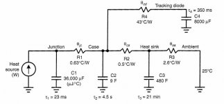
After reading Bob Cordell's book on the thermal model of the TT-devices, I foresee a potential problem caused by thermal attenuation. My previous simulations were based on the assumption that the TT-diodes have the same temperature as the BJT junctions. Regrettably, that is not the case. According to Bob's example (see pic), the thermal x-fer is: (0.5+2.6)/(0.63+0.5+2.6)=0.831. In order to avoid thermal runaway we have to compensate for the thermal resistances. This can be done by amplifying the voltage drop across the TT-diodes by say 20%. But how?
Another possibility is using three TT-diodes for thermal compensation at the expense of giving up the idea of utilizing two TT-diodes (D13 & D14) to create a low impedance between the emitters of the driver as posted here: http://www.diyaudio.com/forums/solid-state/174218-rebirth-phoenix-3.html#post2336489
So, I'm waiting for the right inspiration to find an elegant solution without sacrificing other nice features.
Cheers,
E.
Hi Arthur,
After reading Bob Cordell's book on the thermal model of the TT-devices, I foresee a potential problem caused by thermal attenuation. My previous simulations were based on the assumption that the TT-diodes have the same temperature as the BJT junctions. Regrettably, that is not the case. According to Bob's example (see pic), the thermal x-fer is: (0.5+2.6)/(0.63+0.5+2.6)=0.831. In order to avoid thermal runaway we have to compensate for the thermal resistances. This can be done by amplifying the voltage drop across the TT-diodes by say 20%. But how?
Another possibility is using three TT-diodes for thermal compensation at the expense of giving up the idea of utilizing two TT-diodes (D13 & D14) to create a low impedance between the emitters of the driver as posted here: http://www.diyaudio.com/forums/solid-state/174218-rebirth-phoenix-3.html#post2336489
So, I'm waiting for the right inspiration to find an elegant solution without sacrificing other nice features.
Cheers,
E.
Attachments
Vbe multiplier capaciatance to heatsink
Hello Edmond
I did some simple measurements of the capacitance of the Vbe multiplier to get a handle of the magnitude of the capacitance involved . I used a 2SC5171( TO220) as the VBE transistor.
Connected directly to a large heatsink the capacitance between the 2SC5171(all legs shorted) and the large heat sink was 17pf, with the 2SC5171 mounted on top of a 2SC2922( power transistor) and the heatsink the capacitace is 4.5pf . The second method is what I normally do.
Regards
Arthur
universal front-end
Hi Arthur & Mogens,
See below for a modified front-end, which is more universal in the sense that the standing VAS current isn't any longer defined by the supply current of the op-amp. Now, this current is defined by the diamond buffer following the the op-amp. For test purposes only, the op-amp and OPS has been replaced by a VCVS, E1 respectively E5. So I could simulate the distortion of the discrete part of the front-end, which is pretty low: THD20=72ppb.
This mod costs another two trannies. I hope you don't mind.
You also see a lot of (intimidating) compensation stuff. This is needed because bootstrapped diamond buffers and 'Baxandallized' current mirrors are rather prone to oscillations at very high frequencies.
The next step, the harder part, will be the universal temperature compensation of the OPS. However, I'm still waiting for the right inspiration.
Cheers,
Edmond.
Attachments
The ideas that you are using in your new invention looks like something I have seen before. 
“The next step, the harder part, will be the universal temperature compensation of the OPS. However, I'm still waiting for the right inspiration.”
What kind of inspiration are you and your co-designer looking for?
Have fun
S
“The next step, the harder part, will be the universal temperature compensation of the OPS. However, I'm still waiting for the right inspiration.”
What kind of inspiration are you and your co-designer looking for?
Have fun
S
OPS bias
Probably, you mean some of my previous designs.
Or do mean someone else's design? If so, you certainly can drop a link to that.
Something that really works:
1. An arrangement that isn't overcompensated neither under-compensated.
2. An OPS bias current that doesn't depend on the supply voltage.
3. An OPS bias current that doesn't depend on the standing VAS current.
4. A circuit that doesn't (also capacitively!) load the VAS output cq. driver input.
5. A circuit, including the PCB, that can easily be adopted to ThermalTrack and TT-less output trannies.
6. A circuit that doesn't steal precious Volts from the VAS.
As you see, easy to fulfill requirements. So I'm sure you can and will help us with some bright idea.
edit: one more point added.
The ideas that you are using in your new invention looks like something I have seen before.
Probably, you mean some of my previous designs.
Or do mean someone else's design? If so, you certainly can drop a link to that.
“The next step, the harder part, will be the universal temperature compensation of the OPS. However, I'm still waiting for the right inspiration.”
What kind of inspiration are you and your co-designer looking for?
Have fun
S
Something that really works:
1. An arrangement that isn't overcompensated neither under-compensated.
2. An OPS bias current that doesn't depend on the supply voltage.
3. An OPS bias current that doesn't depend on the standing VAS current.
4. A circuit that doesn't (also capacitively!) load the VAS output cq. driver input.
5. A circuit, including the PCB, that can easily be adopted to ThermalTrack and TT-less output trannies.
6. A circuit that doesn't steal precious Volts from the VAS.
As you see, easy to fulfill requirements. So I'm sure you can and will help us with some bright idea.
edit: one more point added.
Last edited:
Biased inpiration.
Hi Arthur & Mogens,
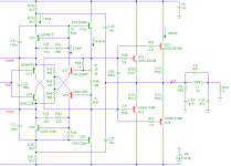
Here's the bias circuit for the Sanken trannies (thus without TT-diodes), see 1st pic.
For temperature sensing I've used rather heavy driver trannies (Q16 & Q17) operation under a relative low collector current (0.6mA). Under this condition the Vbe tempco is about 30% higher than the tempco of Sankens. Probably this is just enough to compensate for the thermal attenuation.
Partly because the DC loop gain of the bias circuit is pretty high (67dB, due to Q15), partly because the base voltage of the output devices is directly sensed, the bias current is insensitive to the operating conditions of the drivers and supply voltage. The only thing that has some influence is the Early effect of the OP devices, See 2nd pic. I hope you can live with that.
As the loop gain is quite high, great care has to be taken to ensure a decent roll-off at HF. Almost all shown capacitors have an effect, though C24 & R38 fulfill a major role in this respect. See 3rd pic. PM=73degrees and GM=24dB.
C25 & C27 represent the collector-heat sink capacitance of Q16 respectively Q17 (17pF). It seems that they don't do any harm.
Perhaps you wonder why the asymmetry: D1 versus Q15. Replacing D1 by a tranny in the same way as Q15 doesn't work, as one of them will saturate. (As you know, because you can't put two current sources in series)
So this was the first hurdle. Now the next one: the integration of the TT-diodes, if possible altogether....
Maybe Stinius has a brilliant idea.
Cheers,
E.
Hi Arthur & Mogens,
Here's the bias circuit for the Sanken trannies (thus without TT-diodes), see 1st pic.
For temperature sensing I've used rather heavy driver trannies (Q16 & Q17) operation under a relative low collector current (0.6mA). Under this condition the Vbe tempco is about 30% higher than the tempco of Sankens. Probably this is just enough to compensate for the thermal attenuation.
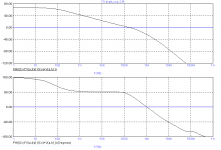
Partly because the DC loop gain of the bias circuit is pretty high (67dB, due to Q15), partly because the base voltage of the output devices is directly sensed, the bias current is insensitive to the operating conditions of the drivers and supply voltage. The only thing that has some influence is the Early effect of the OP devices, See 2nd pic. I hope you can live with that.
As the loop gain is quite high, great care has to be taken to ensure a decent roll-off at HF. Almost all shown capacitors have an effect, though C24 & R38 fulfill a major role in this respect. See 3rd pic. PM=73degrees and GM=24dB.
C25 & C27 represent the collector-heat sink capacitance of Q16 respectively Q17 (17pF). It seems that they don't do any harm.
Perhaps you wonder why the asymmetry: D1 versus Q15. Replacing D1 by a tranny in the same way as Q15 doesn't work, as one of them will saturate. (As you know, because you can't put two current sources in series)
So this was the first hurdle. Now the next one: the integration of the TT-diodes, if possible altogether....
Maybe Stinius has a brilliant idea.
Cheers,
E.
Attachments
Last edited:
The ideas that you are using in your new invention looks like something I have seen before.
“The next step, the harder part, will be the universal temperature compensation of the OPS. However, I'm still waiting for the right inspiration.”
What kind of inspiration are you and your co-designer looking for?
Have fun
S
At best, that s trolling...
At worst, it didn t deserve a (long) comment..
symmetrical bias circuit
As I'm a believer in symmetry, I couldn't resist the temptation to also investigate a fully complementary version of the bias circuit. So I replaced the diode by one more tranny and (of course) some frequency compensating stuff. Initially, I had issues with balancing Vce of Q15 and Q16, though the solution appears to be quite simple: by means of feedback via R38 and R40.
Also, there was another issue: Ic of Q17 and Q18 is not constant, as it is determined by Vbe of Q15, respectively Q16, (divided by 1k) which in turn depends on Tamb. By cross-connecting the emitters of Q18 & Q18 to R39 the dependence on Tamb is reduced to ~0.04%/K (thus negligible).
The (necessary) amount of overcompensation is slightly more: ~40% compared to 30% of the previous circuit. Not a serious problem, as it can be easily adjusted. Moreover, better safe than sorry.
Some key figures of the bias loop: DC gain = 69dB; PM = 87 deg @ 110kHz and GM = 22dB @ 790kHz.
BTW, THD20 dropped by ~7dB. Now it's ~0.7ppm (BW=200kHz). I don't know why. Let's hope it's not a simulation artifact.
Cheers,
E.
Hi Arthur & Mogens,
.................
Perhaps you wonder why the asymmetry: D1 versus Q15. Replacing D1 by a tranny in the same way as Q15 doesn't work, as one of them will saturate. (As you know, because you can't put two current sources in series)
................
As I'm a believer in symmetry, I couldn't resist the temptation to also investigate a fully complementary version of the bias circuit. So I replaced the diode by one more tranny and (of course) some frequency compensating stuff. Initially, I had issues with balancing Vce of Q15 and Q16, though the solution appears to be quite simple: by means of feedback via R38 and R40.
Also, there was another issue: Ic of Q17 and Q18 is not constant, as it is determined by Vbe of Q15, respectively Q16, (divided by 1k) which in turn depends on Tamb. By cross-connecting the emitters of Q18 & Q18 to R39 the dependence on Tamb is reduced to ~0.04%/K (thus negligible).
The (necessary) amount of overcompensation is slightly more: ~40% compared to 30% of the previous circuit. Not a serious problem, as it can be easily adjusted. Moreover, better safe than sorry.
Some key figures of the bias loop: DC gain = 69dB; PM = 87 deg @ 110kHz and GM = 22dB @ 790kHz.
BTW, THD20 dropped by ~7dB. Now it's ~0.7ppm (BW=200kHz). I don't know why. Let's hope it's not a simulation artifact.
Cheers,
E.
Attachments
Last edited:
I received a question about the cross-conduction. To get an idea of the relative performance, I followed the same procedure as here: http://www.diyaudio.com/forums/solid-state/174218-rebirth-phoenix-3.html#post2336489, i.e. an input of 200kHz and 1.4V.
Compared to the former version, the cross-conduction is slightly higher: 530mA and 345mA at the positive-going transition, respectively negative-going transition. Admittedly, this is far more than the idle Iq of 100mA, thought I don't think it's dangerous. Besides, 200 kHz at almost full power is an extreme test condition, which will never occur in real life.
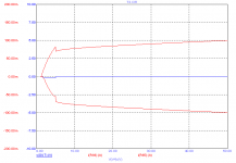
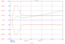
I also had a look at the bias during startup, see 2nd pic. Around a supply voltage of 5V the bias current peaks to about three times its nominal value. This peak has something to do with the crosswise connection of the emitters of Q18 & Q18 to R39 (if R39=0 the peaking has gone). At the moment I don't bother to do something about it, as the power dissipation (per power tranny) at this peak (see green curve) is still far below the idle value of 5 Watt. Moreover, above 12V the bias is remarkable stable. So if it works, don't fix it.
Cheers,
E.
Compared to the former version, the cross-conduction is slightly higher: 530mA and 345mA at the positive-going transition, respectively negative-going transition. Admittedly, this is far more than the idle Iq of 100mA, thought I don't think it's dangerous. Besides, 200 kHz at almost full power is an extreme test condition, which will never occur in real life.
I also had a look at the bias during startup, see 2nd pic. Around a supply voltage of 5V the bias current peaks to about three times its nominal value. This peak has something to do with the crosswise connection of the emitters of Q18 & Q18 to R39 (if R39=0 the peaking has gone). At the moment I don't bother to do something about it, as the power dissipation (per power tranny) at this peak (see green curve) is still far below the idle value of 5 Watt. Moreover, above 12V the bias is remarkable stable. So if it works, don't fix it.
Cheers,
E.
Attachments
- Status
- This old topic is closed. If you want to reopen this topic, contact a moderator using the "Report Post" button.
- Home
- Amplifiers
- Solid State
- Rebirth of the Phoenix