>As for TT-trannies: How large is VBE of the TT-trannies WRT VFWD of the TT-diodes?
I just simmed a simple test circuit and it seemed that VFWD of the NJL4281/4302 diodes tracks VBE NJL1302/3281 trannies reasonably well. Let's hope the same applies to the NJL4281/4302 trannies.
This is one of the things that has to be confirmed by real measurements.
Arthur, could you do this, please?
Cheers,
E.
Attachments
Edmond's bias is quite different from Roender's
Roender shows 5 diodes with a low current through them. This forced us to adopt a 3pair output stage.
Whereas Edmond shows 2 diodes with a high current through them. {Suits a 1pair build, but not 2pair nor more.}
becomes {Suits a 2pair build, but not 3pair nor more}
Edit.
Edmond's next post explains why 2pair suits his biasing topology.
Last edited:
two pairs
Hi Arthur,
Regarding the test circuit, of course that's okay. However, regarding the final version, you need two pairs for two reasons:
1. In order to not exceed the SOA.
2. We need a 2nd pair of TT-diodes (D13 & D14) in order to avoid cross-conduction of the O/P devices. Please see my previous post on this: http://www.diyaudio.com/forums/solid-state/174218-rebirth-phoenix.html#post2320477
In one of my next comments I will elaborate on this and make clear why a simple R and C between the bases of NPN and PNP output devices is essentially totally wrong.
Cheers,
E
Hello Edmond
Is it ok to build it with one pair (1*NPN and 1*PNP ) or do I need 2 pairs as drawn above.
Regards
Arthur
Hi Arthur,
Regarding the test circuit, of course that's okay. However, regarding the final version, you need two pairs for two reasons:
1. In order to not exceed the SOA.
2. We need a 2nd pair of TT-diodes (D13 & D14) in order to avoid cross-conduction of the O/P devices. Please see my previous post on this: http://www.diyaudio.com/forums/solid-state/174218-rebirth-phoenix.html#post2320477
In one of my next comments I will elaborate on this and make clear why a simple R and C between the bases of NPN and PNP output devices is essentially totally wrong.
Cheers,
E
Hi Edmond
As its drawn the bias current is 103 ma per device, with one pair of output the bias current is 113 ma per device according to the simulator.
>We need a 2nd pair of TT-diodes (D13 & D14) in order to avoid cross-conduction of the O/P devices.
I follow the reasoning for this namely to maintain low impedence between the emitters at high frequencies so these drivers can operate in push pull. This is a nice use of the additional TT diodes.
Regards
Arthur
cross-conduction
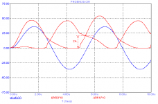
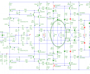
Now, let's fiddle with the stuff between the bases of NPN and PNP output devices and see what happens if we apply a 200kHz sine wave. Admittedly, a rather high frequency, but it makes perfectly clear that essentially there are cross-conduction issues.
1. If no C13 (100nF), no diodes (D13 & D14), only R49=220 Ohms: After only cycle the bias rose from 100mA to 2A, see 1st pic. Needless to say that this is totally unacceptable.
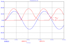
To remedy this nasty habit of BJTs (and sloppy drivers), almost invariably a speed-up capacitor is placed between the bases of NPN and PNP output devices. It cures the trouble, but not for long, as the cap get overcharged after a few cycles. As a result, the bias of the O/P devices increases and equally worse, the bias of driver decreases. See 2nd pic (C13=100nF & R49=220 Ohms).
BTW, in some cases, the decrease of the driver bias may even lead to HF instability (probably, this was the case with a precursor of syn08's YAP).
This is the reason why in some of my designs I'm using two separate push-pull drivers, one for the top O/P devices and one for the bottom O/P devices and no cross-coupled cap at all.
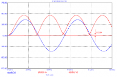
However, a far more elegant and simple solution is to make clever use of the matched TT diodes, which provides a low and frequency independent impedance between the emitters of the drivers. Now both of them can sink and source enough current to turn off the O/P trannies more quickly. With C13=100nF, R49=2.2R and the TT-diodes installed, the increase in bias current is far less, only 150mA. See 3rd pic.
Apart from more power, that's why I strongly recommend to use two pairs of NJL4281/4302, i.e two TT-diodes for biasing and two TT-diodes for fast turn-off (btw, no 3281/1302, as these trannies have different and less suitable diodes).
Cheers,
E.
edit: apparently we cross-posted.
Now, let's fiddle with the stuff between the bases of NPN and PNP output devices and see what happens if we apply a 200kHz sine wave. Admittedly, a rather high frequency, but it makes perfectly clear that essentially there are cross-conduction issues.
1. If no C13 (100nF), no diodes (D13 & D14), only R49=220 Ohms: After only cycle the bias rose from 100mA to 2A, see 1st pic. Needless to say that this is totally unacceptable.
To remedy this nasty habit of BJTs (and sloppy drivers), almost invariably a speed-up capacitor is placed between the bases of NPN and PNP output devices. It cures the trouble, but not for long, as the cap get overcharged after a few cycles. As a result, the bias of the O/P devices increases and equally worse, the bias of driver decreases. See 2nd pic (C13=100nF & R49=220 Ohms).
BTW, in some cases, the decrease of the driver bias may even lead to HF instability (probably, this was the case with a precursor of syn08's YAP).
This is the reason why in some of my designs I'm using two separate push-pull drivers, one for the top O/P devices and one for the bottom O/P devices and no cross-coupled cap at all.
However, a far more elegant and simple solution is to make clever use of the matched TT diodes, which provides a low and frequency independent impedance between the emitters of the drivers. Now both of them can sink and source enough current to turn off the O/P trannies more quickly. With C13=100nF, R49=2.2R and the TT-diodes installed, the increase in bias current is far less, only 150mA. See 3rd pic.
Apart from more power, that's why I strongly recommend to use two pairs of NJL4281/4302, i.e two TT-diodes for biasing and two TT-diodes for fast turn-off (btw, no 3281/1302, as these trannies have different and less suitable diodes).
Cheers,
E.
edit: apparently we cross-posted.
Attachments
Last edited:
Hi Andrew,
You're welcome.
Hi Arthur,
The current model of the TT-diode is misleading, as the TC is too high. By changing EG, IS and N (changing XTI had no effect) I have lowered the TC down to 1.7mV/K (as it ought to be).
Old model:
.MODEL TTdiode-old D (
+ IS=5.5e-008 RS=0.65 N=2 TT=5.1937e-008 CJO=2.08272e-011 VJ=1.5
+ M=0.653713 EG=1.3 XTI=2.33354 BV=400 IBV=1e-005 )
New model:
.MODEL TTdiode D (
+ IS=1.2e-009 RS=0.65 N=1.5 TT=5.1937e-008 CJO=2.08272e-011 VJ=1.5
+ M=0.653713 EG=1.05 XTI=2.33354 BV=400 IBV=1e-005 )
With this new model the amp is slightly undercompenated (as expected). So I have to mend this shortcoming by means of some additional TC stuff.
I will soon drop a new schematic that also compensates for the Ibias dependence of Vcc and Vee.
Cheers,
E.
Stuff
Hello Edmond
With regards to the NJL4281/4302DG parts I am waiting for delivery of these from overseas the US as there is no local stock it should take 6 days at the most.
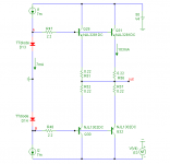
I would like to ask you about C16, C17 and R16 and R17 see attachment where did you put the gain probe to get these values.
I can only speak for myself but I enjoy your explanation and simulations that you do to explain technical matters you have a pedagogic style.
Thanks also for the new TT diode model, who made the old model.
Regards
Arthur
Hello Edmond
With regards to the NJL4281/4302DG parts I am waiting for delivery of these from overseas the US as there is no local stock it should take 6 days at the most.
I would like to ask you about C16, C17 and R16 and R17 see attachment where did you put the gain probe to get these values.
I can only speak for myself but I enjoy your explanation and simulations that you do to explain technical matters you have a pedagogic style.
Thanks also for the new TT diode model, who made the old model.
Regards
Arthur
Attachments
Last edited:
Hello Edmond
With regards to the NJL4281/4302DG parts I am waiting for delivery of these from overseas the US as there is no local stock it should take 6 days at the most.
Hi Arthur,
Great! BTW, did you already get the 2SK150s ?
I would like to ask you about C16, C17 and R16 and R17 see attachment where did you put the gain probe to get these values.
At R16 and R17, that, is a Middlebrook gain probe. Discussing this subject is on my todo list, but may I suggest that we do this after the bias topic is finished.
I can only speak for myself but I enjoy your explanation and simulations that you do to explain technical matters you have a pedagogic style.
Thanks you.
Thanks also for the new TT diode model, who made the old model.
Regards
Arthur
The model originates from MODPEX and modified by Andy_C and/or Bob Cordell.
Cheers,
Edmond.
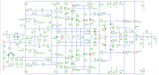
OPS bias
Hi Arthur,
More on OPS bias. As said before, with the new diode models it appears that the temperature compensation is not adequate enough:
T= -37ºC Ibias = 78mA
T= +27ºC Ibias = 99mA
T= +77ºC Ibias = 117mA
So we need a bit more compensation. By means of a third TT-diode? There are no TT-diodes left over. Moreover, a third diode will make the circuit overcompensated. Something similar to a Vbe-multiplier isn't feasible either, at least not with this kind of topology.
So I decided to make the current sources that feed the TT-diodes temperature dependent. This is relative easy, see below, Q15, Q16, Q17 & Q20.
Q16 & Q17 are mounted on the same heat sink as the O/P trannies.
Now the temperature tracking is almost perfect, though still slightly under-compensated. Therefore I added R40 & R41 in order to increase the TC. I got the following results:
T= -37ºC Ibias = 93mA
T= +27ºC Ibias = 99mA
T= +77ºC Ibias = 93mA
Not that bad, I would say.")
It should be noted that in real life you might need higher values for R40 & R41 and, as a consequence, you also might need a negative voltage between the bases of Q18 & Q19 (by crosswise connecting them to trim pot P1).
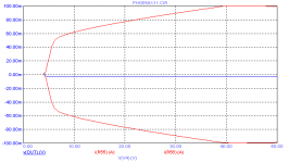
Next, we have one more bias issue: the dependence on the supply voltage. With the new current sources this problem is quite easy to resolve: simply by stealing some current from the aforementioned CCSes with rising supply voltage. Basically, this can be done with one resistor between the emitters of Q17 and Q20. But we don't need compensation along the whole trajectory from 0 to 50V. It is sufficient to compensate for the last 10 Volts or so (i.e. from 40 to 50V). Such scheme saves power and minimizes the loss of voltage swing of the CCSes. (Q19 & Q20 are the first trannies that will saturate at clipping)
So I put a zener in series with the resistor. In the schematic below you see two of them and two resistors: D10, D11, R37 & R38, instead of only one. This has been done for two reasons: To limit the dissipation in each of these components and to ease the layout of the PCB, i.e. to use them as 'jumpers' as well.
See second pic for the results. Between 40 and 50V the bias is almost constant.
Again, it should be noted that in real life you might need other values for R37 & R38.
Cheers,
E.
PS1: Notice that I have replaced Q18 and Q19 by a KSA1220A, respectively KSC2690A for better temp. tracking, lower Vbe AND a lower ULG frequency of the Miller loop. The choice of these trannies (and the value of R45 & R46) has a profound effect on the Miller-ULGF! More on this later on.
PS2: You can change the temp. of the red encircled components by changing the following line on the text page: .define TA 27 ; Temp. TT devices and Q15, Q16
PS3: I also have added D5 in order to reduce the effect of VAS current variations.
Hi Arthur,
More on OPS bias. As said before, with the new diode models it appears that the temperature compensation is not adequate enough:
T= -37ºC Ibias = 78mA
T= +27ºC Ibias = 99mA
T= +77ºC Ibias = 117mA
So we need a bit more compensation. By means of a third TT-diode? There are no TT-diodes left over. Moreover, a third diode will make the circuit overcompensated. Something similar to a Vbe-multiplier isn't feasible either, at least not with this kind of topology.
So I decided to make the current sources that feed the TT-diodes temperature dependent. This is relative easy, see below, Q15, Q16, Q17 & Q20.
Q16 & Q17 are mounted on the same heat sink as the O/P trannies.
Now the temperature tracking is almost perfect, though still slightly under-compensated. Therefore I added R40 & R41 in order to increase the TC. I got the following results:
T= -37ºC Ibias = 93mA
T= +27ºC Ibias = 99mA
T= +77ºC Ibias = 93mA
Not that bad, I would say.
It should be noted that in real life you might need higher values for R40 & R41 and, as a consequence, you also might need a negative voltage between the bases of Q18 & Q19 (by crosswise connecting them to trim pot P1).
Next, we have one more bias issue: the dependence on the supply voltage. With the new current sources this problem is quite easy to resolve: simply by stealing some current from the aforementioned CCSes with rising supply voltage. Basically, this can be done with one resistor between the emitters of Q17 and Q20. But we don't need compensation along the whole trajectory from 0 to 50V. It is sufficient to compensate for the last 10 Volts or so (i.e. from 40 to 50V). Such scheme saves power and minimizes the loss of voltage swing of the CCSes. (Q19 & Q20 are the first trannies that will saturate at clipping)
So I put a zener in series with the resistor. In the schematic below you see two of them and two resistors: D10, D11, R37 & R38, instead of only one. This has been done for two reasons: To limit the dissipation in each of these components and to ease the layout of the PCB, i.e. to use them as 'jumpers' as well.
See second pic for the results. Between 40 and 50V the bias is almost constant.
Again, it should be noted that in real life you might need other values for R37 & R38.
Cheers,
E.
PS1: Notice that I have replaced Q18 and Q19 by a KSA1220A, respectively KSC2690A for better temp. tracking, lower Vbe AND a lower ULG frequency of the Miller loop. The choice of these trannies (and the value of R45 & R46) has a profound effect on the Miller-ULGF! More on this later on.
PS2: You can change the temp. of the red encircled components by changing the following line on the text page: .define TA 27 ; Temp. TT devices and Q15, Q16
PS3: I also have added D5 in order to reduce the effect of VAS current variations.
Attachments
Last edited:
Hi Arthur,
By adding the variable T_ABS to the model parameters and assign a temperature to this variable via a global definition.
In phoenix11.cir this is .define TA 27 for example.
BTW, the acronym 'T_ABS' is a bit misleading, as it is NOT the absolute temperature in Kelvin, rather it is 'absolute' in the sense that it is not changed by other temperature definitions, like the temperature in the so called 'limits dialog boxes'.
.MODEL TTdiode D ( IS=1.2e-009 RS=0.65 N=1.5 TT=5.1937e-008 CJO=2.08272e-011
+ VJ=1.5 M=0.653713 EG=1.05 XTI=2.33354 BV=400 IBV=1e-005 T_ABS=TA )
.MODEL KSA1220TT PNP (BF=289.3 BR=9.76 CJC=1.1224E-10 CJE=3.4786E-10 EG=1.2255
+ FC=0.5 IKF=2.7061 IKR=0.0759 IRB=0.001 IS=4.7863E-13 ISC=2.4909E-11
+ ISE=5.2481E-12 MJC=0.4365 MJE=0.4694 NC=1.5 NE=2 NF=1.0 NR=1.006 RB=2.26
+ RBM=0.2308 RC=1.1748 RE=0.1908 T_ABS=TA VAF=98.5 VAR=6.7 VJC=0.5761
+ VJE=0.9575 XCJC=0.4955 XTB=1.7978 XTI=3.0)
etc. etc
Cheers,
E.
Clamp
Hi Arthur,
Good question.
If I had not crosswise connected this stuff (as in phoexix5), the maximum clamp feedback current is limited by the current sources (Q17 resp. Q20, 7mA) This is not enough under worst case conditions. With Phoenix5 this wasn't an issue, as the pre-drivers could source resp. sink enough current. In later versions however, the double EF driver has been replaced by a diamond buffer. Now the 'top' pre-driver, for example, is a PNP tranny (instead of NPN), which can't source any current at all, only the top CCS can do this. That's the problem, well, actually a small problem. Therefore, I've (cross) connected the 'top' clamp stuff to the 'bottom' pre-driver. Being a NPN, the emitter of this tranny can source plenty of current. The same applies of course to the 'bottom' clamp stuff and the 'top' pre-driver.
That's all. No esoteric hocus-pocus.
Note that the zener voltage of D6 & D7 has been increased accordingly.
Cheers,
E.
Hello Edmond
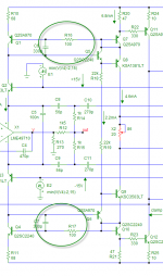
In the Pheonix11 why do you cross the connection of the of the emitters of the clamping circuitry of Q13 and Q14 as shown in the attachment.
Regards
Arthur
Hi Arthur,
Good question.
If I had not crosswise connected this stuff (as in phoexix5), the maximum clamp feedback current is limited by the current sources (Q17 resp. Q20, 7mA) This is not enough under worst case conditions. With Phoenix5 this wasn't an issue, as the pre-drivers could source resp. sink enough current. In later versions however, the double EF driver has been replaced by a diamond buffer. Now the 'top' pre-driver, for example, is a PNP tranny (instead of NPN), which can't source any current at all, only the top CCS can do this. That's the problem, well, actually a small problem. Therefore, I've (cross) connected the 'top' clamp stuff to the 'bottom' pre-driver. Being a NPN, the emitter of this tranny can source plenty of current. The same applies of course to the 'bottom' clamp stuff and the 'top' pre-driver.
That's all. No esoteric hocus-pocus.
Note that the zener voltage of D6 & D7 has been increased accordingly.
Cheers,
E.
Hello Edmond
>Great! BTW, did you already get the 2SK150s ?
By this do you mean 2SK1530 , I just confirmed that they now have them in stock (Y selection) but I have not got them yet as yet. Did you purchase any from the guys I recommended.
Regards
Arthur
Not yet, but I will do it very soon.
They also have 2SJ201, don't they?
Cheers,
E.
- Status
- This old topic is closed. If you want to reopen this topic, contact a moderator using the "Report Post" button.
- Home
- Amplifiers
- Solid State
- Rebirth of the Phoenix