Does anyone have any of these boards laying arond for sale? I would buy 3-4 dozen of them if I could. I would hope to hear from Owen, but assume he has no longer been buidling these or selling. I wish the PCB design would be open for use of the public. I would sell these If I could get permission from Owen. Has anyone talked with him recently?
This is such a great design and sadly hate to see this not be put to good use.
This is such a great design and sadly hate to see this not be put to good use.
I picked up a curve tracer to make transconductance testing and matching easier and should have some results soon. Since setting Vds correctly is important for the curve tracer measurements, I wanted to double check that my calculations are correct.
With Rs = 7, Rd = 2.8, and supply rail of +/-6V, current through the MOSFET is (1.65 + 6)/7 = 1.0929A. Then using the drain-source loop KVL, 6 - (7 * Id) - Vds - (2.8 * Id) = -6, so Vds = 12 - (9.8 * 1.0929) = 1.29V
This checks out since you're biasing at the source for the 1.65V DAC offset and Vd = 6 - (1.0929 * 2.8) = 2.94V, so Vds = 2.94 - 1.65 = 1.29V.
LTSpice seems to confirm this is correct, but let me know if I've made any mistakes.
I measured the transconductance of the following logic-level MOSFETs at 1.09A and IRL1404S came out on top at almost 14S.
It's interesting that LTspice distortion simulations don't really correlate with transconductance. I wonder if that's due to simulation and/or model quality and the lack of subthreshold parameters, or if there are other MOSFET characteristics that affect NTD1 distortion measurements other than transconductance.
It's interesting that LTspice distortion simulations don't really correlate with transconductance. I wonder if that's due to simulation and/or model quality and the lack of subthreshold parameters, or if there are other MOSFET characteristics that affect NTD1 distortion measurements other than transconductance.
Code:
[B]Model	        Transconductance[/B]
IRL1404S	13.9810852
IRL2505S	12.0627706
IRL60S216	11.9672906
IRL3705NS	10.9092788
IRL2203NS	10.2643684
FQB34N20LTM	9.9900624
IRL3713S	9.239449
IRL2910S	9.172273
IRL3803S	8.990884
FQB50N06LTM	8.554364
FQB19N20LTM	8.452541
IRL3103S	8.423891
IRL40S212	8.393629
FQB33N10LTM	8.125394
IRLZ44NS	7.99665
IRL540NS	7.871818
IRLZ34NS	7.082997
FQB30N06LTM	6.194258
IRLZ24NS	5.799751
IRL530NS	5.581292
IRL520NS 4.230913Also looking for a SE-SE board, BAL-BAL board. 1x PSU PCB and 1x LT3042 parallel regulator PCB.
I have an assembled SE-SE and an assembled PSU board if that's interesting.
Phono Board shorting issues?
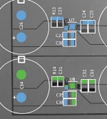
Through the kindness of a fellow DIYer I was able to get a phono board, and when it arrived I was concerned about the way the pads looked at the2 regulators. I think they're fine, but there is what I think a real problem. I've attached a photo of the board that has the 4 grounds color coded, and where they happen across the board. Note C26, which has both legs connected—this of course ends up affecting things all over the place. (I'm not saying that the problem is right at C26; it could be many places, and this is one of my questions.)
Is this correct? I don't understand how it could be, but I am self trained, and will be the first to admit my lack of understanding. I assume that the Caps all connected to the V+ on the INAs are shorted based on this also, but if not, would love an explanation about how they work that way.
Note that The grounds on both audio legs are shorted—I was testing across as 4 separate areas, but basically, anything marked magenta is also orange, and vise versa. But I kept these 4 colors going thinking it might make it easier to discuss.
So, if any of you either have specific experience with this board or can just explain what is happening (even better if you can suggest a trouble shooting process) I'd really appreciate it. I can send close ups of the board if that will help. I'd really like to build this project.
Attachments
Last edited:
Hi Picovolt,
I'm impressed that you took the time to check the board for shorts before building! That's the sort of thing I always tell myself to do before building a prototype board for the first time, but then I get too excited and just build it. That has caught me out more times than one would expect")
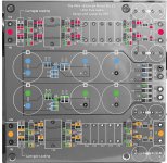
In this case though, I can assure you the PCB is fine. The part that is throwing you for a loop is that I use two positive regulators to generate a bipolar supply. This is possible because the dual secondaries of the transformer are isolated from one another, and that isolation remains all the way until the output of the regulators where I use one normally, and the other has its "output" tied to GND and its "GND" becomes the negative rail. If you take a look at the schematic, this may make more sense.
Also attached here is screen shot if the PCB layout without the power planes poured. Hopefully it will help you make more sense of things. I always colour code the nets when I'm routing as it makes things visually easier.
Take a look and see if it makes sense. I always build and test a board from every batch, so it's extremely unlikely that your PCB is not correct.
Regards,
Owen
I'm impressed that you took the time to check the board for shorts before building! That's the sort of thing I always tell myself to do before building a prototype board for the first time, but then I get too excited and just build it. That has caught me out more times than one would expect
In this case though, I can assure you the PCB is fine. The part that is throwing you for a loop is that I use two positive regulators to generate a bipolar supply. This is possible because the dual secondaries of the transformer are isolated from one another, and that isolation remains all the way until the output of the regulators where I use one normally, and the other has its "output" tied to GND and its "GND" becomes the negative rail. If you take a look at the schematic, this may make more sense.
Also attached here is screen shot if the PCB layout without the power planes poured. Hopefully it will help you make more sense of things. I always colour code the nets when I'm routing as it makes things visually easier.
Take a look and see if it makes sense. I always build and test a board from every batch, so it's extremely unlikely that your PCB is not correct.
Regards,
Owen
Attachments
- Home
- Vendor's Bazaar
- "The Wire" Official Boards for All Projects Available Here! BAL-BAL, SE-SE, LPUHP