My understanding (and a quick sim for a different length)
indicates that Klaus's results match mine - I get a similar
set of resonances. The problem remains - what's the deal with
Polk "Cobra" cable and the relative dielectric?
😎
indicates that Klaus's results match mine - I get a similar
set of resonances. The problem remains - what's the deal with
Polk "Cobra" cable and the relative dielectric?
😎
anatech said:Hi Ovidiu,
I think we are in complete agreement here. One reason DiyAudio even exists.
Now that is an interesting point. Perhaps National may incorporate that into some of their driver chips or complete amp assy's. They are putting a large effort into cornering the audio market on every level, wouldn't you say?
-Chris
Edit: TI is also in there fighting for market share.
Hi Chris,
I spent several hours with the National guys at the recent AES Convention in NY. These guys are dead serious, and have a very good story to tell. They had a very good demonstration setup using amplifiers and preamps built with their new ICs and driving hi-end speaker systems, and it sounded very good. Thay have an outstanding fully complementary bipolar process. They also have an unusually keen idea of high-end audio issues apart from mere specs that we often do not see in IC companies.
Cheers,
Bob
Re: Re: Re: Re: Is error correction inconvenient?
Ovidiu,
Thanks very much for these models. Do you by chance also have the models for the 2SC3421/2SA1358 TO-126 devices you used?
I'll look forward to your open-loop, no-EC output stage THD-20 measurements (but I do realize you are very busy; I've also been getting hammered at work lately).
You're certainly right about other parts of the EC circuit interacting with and affecting the HEC balance condition, especially in very simple HEC implementations. However, the gm of the error stage transistors will be quite predictable and repeatable, since it is mainly determined by emitter operating current, rather than emitter area. Obviously, this assumes that ohmic emitter resistance and base resistances are small enough in a relative sense to be of little consequence. Good transistors in the EC circuit, especially with high beta and ft, help a lot. Also, if one makes the error stage transistors into CFPs, this can help a lot both with the current gain issue and the transconductance issue.
Cheers,
Bob
Thanks!
Bob
syn08 said:Bob,
What was your open-loop output stage THD-20 without EC? This helps give me a calibration, since I believe that in my amp the EC dropped the THD-20 by about a factor of 30.
Unfortunately I don't know precisely. I haven't in particular measured this, but I may do it ASAP. All I seem to recall is the open loop THD20 with the EC grossly mistuned, about 0.12% at 10V output for the same Ibias= 150mA/device.
I probably have not thought about it hard enough, but I am surprized to hear you assert that the proper balance and optimum performance of the HEC circuit depends on absolute resistor values as opposed to just relative matching precision. Perhaps you only meant the term matching in regard to identical pairs of resistor values? Could you elaborate here?
I don't have the time to get into details right now, but very shortly have you ever wondered why the Hawksford balance R1=(1-k)*R2 is not really true in practice, when it comes to the resistor lumped values? Obviously that's because the rest of the circuit is interacting with the balance. These interactions are unfortunately impacting the balance on a "common mode" rather than differential mode. Which means that if you insert a dual pot (as we did) the two optimal values are going to be identical (because the circuit is symetrical) but out of what the Hawksford model predicts. As an example of such a "common mode" imbalance is the emitter areas which are typically +/-10% off and hence Ic can be off by about the same amount, hence rbe can be off by about the same amount. There are other fine points here, like the relative high power dissipation of an EC amp, and hence the high thermal gradient on the chip, hence the need to place the critical resistors on the same izotherm, the need to make the Hawksford balange adjustment bias independent, etc... Of course, one could imagine a EC externally tunable chip, or an on chip tuned resitor process either by laser (as Burr Brown did) or by zener zap (as Analog Devices did). Again, I may be back on this topic. I'll need soon another life to keep track of everything I promised here.
Those are some very nice transistors that you have chosen to use, and I've looked at their spec sheets and am impressed. Can you share with us the SPICE models you used for these transistors?
Here you go. I would really appreciate if andy_c or anybody else would look into these models and further refine them.
.MODEL Q2SA1407 PNP (
+ IS=15.2F
+ NF=1
+ BF=416
+ VAF=254
+ IKF=90M
+ ISE=3.66P
+ NE=2
+ BR=4
+ NR=1
+ VAR=20
+ IKR=.135
+ RE=7.63
+ RB=30.5
+ RC=3.05
+ XTB=1.5
+ CJE=22P
+ VJE=1.1
+ MJE=.5
+ CJC=7.1P
+ VJC=.3
+ MJC=.3
+ TF=397P
+ TR=276N)
.MODEL Q2SC3601 NPN (
+ IS=15.2F
+ NF=1
+ BF=416
+ VAF=254
+ IKF=90M
+ ISE=3.66P
+ NE=2
+ BR=4
+ NR=1
+ VAR=20
+ IKR=.135
+ RE=5.63
+ RB=22.5
+ RC=2.25
+ XTB=1.5
+ CJE=18.3P
+ VJE=1.1
+ MJE=.5
+ CJC=5.91P
+ VJC=.3
+ MJC=.3
+ TF=397P
+ TR=276N)
.MODEL Q2SA1930 PNP(
+ IS=10.000E-15
+ BF=210
+ VAF=78
+ IKF=10.000E-3
+ XTB=1.5
+ BR=.1001
+ VAR=100
+ IKR=10.000E-3
+ ISC=10.000E-15
+ CJE=3.252E-12
+ CJC=63.196E-12
+ MJC=.33333
+ TF=83.239E-12
+ XTF=10
+ VTF=10
+ ITF=1)
.MODEL Q2SC5171 NPN(
+ IS=10.000E-15
+ BF=210
+ VAF=100
+ IKF=10.000E-3
+ XTB=1.5
+ BR=.1001
+ VAR=100
+ IKR=10.000E-3
+ ISC=10.000E-15
+ CJE=2.0000E-12
+ CJC=38.866E-12
+ MJC=.33333
+ TF=83.239E-12
+ XTF=10
+ VTF=10
+ ITF=1)
Ovidiu,
Thanks very much for these models. Do you by chance also have the models for the 2SC3421/2SA1358 TO-126 devices you used?
I'll look forward to your open-loop, no-EC output stage THD-20 measurements (but I do realize you are very busy; I've also been getting hammered at work lately).
You're certainly right about other parts of the EC circuit interacting with and affecting the HEC balance condition, especially in very simple HEC implementations. However, the gm of the error stage transistors will be quite predictable and repeatable, since it is mainly determined by emitter operating current, rather than emitter area. Obviously, this assumes that ohmic emitter resistance and base resistances are small enough in a relative sense to be of little consequence. Good transistors in the EC circuit, especially with high beta and ft, help a lot. Also, if one makes the error stage transistors into CFPs, this can help a lot both with the current gain issue and the transconductance issue.
Cheers,
Bob
Thanks!
Bob
Re: Re: Re: Re: Re: Is error correction inconvenient?
Thanks very much for these models. Do you by chance also have the models for the 2SC3421/2SA1358 TO-126 devices you used?
Those are not critical; I used those trannies only because I have a small stock at hand. For simulation purposes you can use the models for 2SA1220/2SC2690 (this is what I did) listed below:
.MODEL Q2SA1220A PNP ( LEVEL=2
+ IS =4.7863E-13
+ BF =289.3
+ NF =1.0
+ BR =9.76
+ NR =1.006
*+ IBC =4.7863E-13
*+ IBC =4.7863E-13
+ ISE =5.2481E-12
+ NE =2
+ ISC =2.4909E-11
+ NC =1.5
+ VAF =98.5
+ VAR =6.7
+ IKF =2.7061
+ IKR =0.0759
+ RB =2.26
+ RBM =0.2308
+ IRB =0.001
+ RE =0.1908
+ RC =1.1748
+ QCO =0.02
+ RCO =3.9811
+ VO =11.078
+ GAMMA =5.01187E-8
+ CJE =3.4786E-10
+ VJE =0.9575
+ MJE =0.4694
+ FC =0.5
+ CJC =1.1224E-10
+ VJC =0.5761
+ MJC =0.4365
+ XCJC =0.4955
+ XTB =1.7978
+ EG =1.2255
+ XTI =3.0 )
.MODEL Q2SC2690A NPN ( LEVEL=2
+ IS =1.7783E-13
+ BF =132.5
+ NF =1.0
+ BR =8.495
+ NR =1.005
*+ IBC =1.7783E-13
*+ IBC =1.7783E-13
+ ISE =1.9953E-13
+ NE =1.5
+ ISC =1.5849E-9
+ NC =1.98
+ VAF =580.75
+ VAR =18.15
+ IKF =4.0271
+ IKR =0.0120
+ RB =2.98
+ RBM =0.001
+ IRB =0.6396
+ RE =0.0909
+ RC =1.4705
+ QCO =0.68
+ RCO =3.6239
+ VO =6.587
+ GAMMA =2.8216E-7
+ CJE =4.0082E-10
+ VJE =0.6696
+ MJE =0.3296
+ FC =0.5
+ CJC =6.0404E-11
+ VJC =0.5
+ MJC =0.4266
+ XCJC =0.4955
+ XTB =1.2590
+ EG =1.2277
+ XTI =3.0 )
I think Edmond used the 2SB649/2SD669 models in his simulations, those would work as well, without much of a difference.
However, the gm of the error stage transistors will be quite predictable and repeatable, since it is mainly determined by emitter operating current, rather than emitter area.
Of course the gm is determined by the emitter current, however the emitter current is determined by the emitter area. The whole analog IC concept is based on current mirroring and emitter area ratios. As much as you can precisely control resistor ratios, you can precisely control current ratios. However, you can not precisely control (say, to 1%) the absolute current values, unless you employ some sort of on chip trimming technology.
Any chance you'd post anytime soon some details (schematics, etc...) on your distortion magnifier and protection circuit?
Re: Re: Re: Re: Re: Re: Is error correction inconvenient?
Ovidiu,
Thanks for these models.
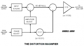
Yes, I'm working on getting both the Distortion Magnifier and protection circuit into electronic format (most of the stuff is hand-drawn on graph paper, I must admit).
For now, here's a peek at the DM block diagram. As you can see, it is not very complicated, but makes a lot of things very convenient. The differential input for the signal from the amplifier under test sometimes helps in keeping noise and pickup down.
Cheers,
Bob
syn08 said:
Thanks very much for these models. Do you by chance also have the models for the 2SC3421/2SA1358 TO-126 devices you used?
Those are not critical; I used those trannies only because I have a small stock at hand. For simulation purposes you can use the models for 2SA1220/2SC2690 (this is what I did) listed below:
.MODEL Q2SA1220A PNP ( LEVEL=2
+ IS =4.7863E-13
+ BF =289.3
+ NF =1.0
+ BR =9.76
+ NR =1.006
*+ IBC =4.7863E-13
*+ IBC =4.7863E-13
+ ISE =5.2481E-12
+ NE =2
+ ISC =2.4909E-11
+ NC =1.5
+ VAF =98.5
+ VAR =6.7
+ IKF =2.7061
+ IKR =0.0759
+ RB =2.26
+ RBM =0.2308
+ IRB =0.001
+ RE =0.1908
+ RC =1.1748
+ QCO =0.02
+ RCO =3.9811
+ VO =11.078
+ GAMMA =5.01187E-8
+ CJE =3.4786E-10
+ VJE =0.9575
+ MJE =0.4694
+ FC =0.5
+ CJC =1.1224E-10
+ VJC =0.5761
+ MJC =0.4365
+ XCJC =0.4955
+ XTB =1.7978
+ EG =1.2255
+ XTI =3.0 )
.MODEL Q2SC2690A NPN ( LEVEL=2
+ IS =1.7783E-13
+ BF =132.5
+ NF =1.0
+ BR =8.495
+ NR =1.005
*+ IBC =1.7783E-13
*+ IBC =1.7783E-13
+ ISE =1.9953E-13
+ NE =1.5
+ ISC =1.5849E-9
+ NC =1.98
+ VAF =580.75
+ VAR =18.15
+ IKF =4.0271
+ IKR =0.0120
+ RB =2.98
+ RBM =0.001
+ IRB =0.6396
+ RE =0.0909
+ RC =1.4705
+ QCO =0.68
+ RCO =3.6239
+ VO =6.587
+ GAMMA =2.8216E-7
+ CJE =4.0082E-10
+ VJE =0.6696
+ MJE =0.3296
+ FC =0.5
+ CJC =6.0404E-11
+ VJC =0.5
+ MJC =0.4266
+ XCJC =0.4955
+ XTB =1.2590
+ EG =1.2277
+ XTI =3.0 )
I think Edmond used the 2SB649/2SD669 models in his simulations, those would work as well, without much of a difference.
However, the gm of the error stage transistors will be quite predictable and repeatable, since it is mainly determined by emitter operating current, rather than emitter area.
Of course the gm is determined by the emitter current, however the emitter current is determined by the emitter area. The whole analog IC concept is based on current mirroring and emitter area ratios. As much as you can precisely control resistor ratios, you can precisely control current ratios. However, you can not precisely control (say, to 1%) the absolute current values, unless you employ some sort of on chip trimming technology.
Any chance you'd post anytime soon some details (schematics, etc...) on your distortion magnifier and protection circuit?
Ovidiu,
Thanks for these models.
Yes, I'm working on getting both the Distortion Magnifier and protection circuit into electronic format (most of the stuff is hand-drawn on graph paper, I must admit).
For now, here's a peek at the DM block diagram. As you can see, it is not very complicated, but makes a lot of things very convenient. The differential input for the signal from the amplifier under test sometimes helps in keeping noise and pickup down.
Cheers,
Bob
Attachments
Nelson Pass said:That's very educational, thank you. I still can't reconcile this
the value for the Polk (Litz type) wire which has an apparent
propagation half that of the Mogami. The capacitance on it
is through the roof at 500 pF/ft, but the material is your standard
"magnet wire" coating. Can the dielectric figure for this enamel
be that high, or is there a geometric dependency?
😎
Remember, that the amount of capacitance/inductance that a signal "sees" is a function of its wavelength. As an extreme case, consider a 1.0 GHz signal with a wavelength on 50 ohm coax of no more than several inches. All capacitance that lies outside of the signal's wavelength is invisible to the signal and does not contribute to the channel's impedance. This is why a properly terminated coaxial cable will display a constant impedance from DC to its cutoff frequency. At DC the impedance is entirely real and defined by the termination resistance. As the frequency increases an ever larger proportion of the impedance is complex and is a function of the per length L and C of the channel. One way to look at the problem is to consider a channel of infinite length with a fixed impedance. If one were to attempt an impedance measurement into such a channel the termination (or lack thereof) at the far end would be immaterial, and only the complex impedance of the channel would matter.
It is easy to estimate the transition point between where a lumped element L/C and a distributed representation of the channel is necessary. It is simply the frequency at which the phase of a signal is not constant over the channel's length. Practically speaking, it is usual to take the 10% point. In other words, if a signal's phase varies by more than 10% over the length of a channel, then it is necessary to evaluate the channel as a distributed, rather than a lumped, network
Re: Distortion Magnifier
Hello Bob,
I'm sure many here are looking forward to more details on the DM! I guess some circuit chunks from your THD analyzer are recycled into the DM 😉 ?
Jan Didden
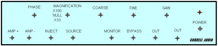
Bob Cordell said:Here's what the front panel looks like.
Cheers,
Bob
Hello Bob,
I'm sure many here are looking forward to more details on the DM! I guess some circuit chunks from your THD analyzer are recycled into the DM 😉 ?
Jan Didden
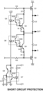
Short Circuit protection circuit
I've posted below a version of the MOSFET short circuit protection that I used in a prototype about a year and a half ago.
Let me first say that the most important thing is the functionality. It is definitely NOT an SOA protection circuit or a current limiter. It is only there to act in the evnt of a short circuit or an event that causes extreme output currents to flow. It is not designed to allow the amplifier to play through the event. Once triggered, it immediately disables the output stage and the amplifier will not operate until the power is cycled. It is intended to be completely non-intrusive during normal operation. Its just a binary thing.
Q1 and Q2 are vertical output MOSFETs with a typical forward gate voltage bias on the order of 3.5 to 4.5 V at idle. Q3 and Q4, once turned on, largely ground the gates to the sources, depriving them of gate drive and shutting the output transistors down. Q3 and Q4 are driven in Darlinton fashion by phototransistors Q5 and Q6.
The protection action is triggered when a large enough voltage appears across the output source resistors. That will turn on the LED in phototransistor Q7. Q7 and Q8 are connected as a positive feedback latch. Once Q7 turns on, it will turn on Q8, which in turn will further turn on and keep on Q7. The current drawn by the Q7-Q8 latch illuminates the phototransistors Q5 and Q6 so as to deprive the output transistors of gate drive.
This circuit, as shown, would need to probably be modified to work with lower-threshold V MOSFETs and may not be suitable without considerable modification for lateral MOSFETs. I like this circuit because of its isolation with phototransistors, as the latch/control circuit is referenced to circuit ground, rather than floating with the audio signal. This allows for other interesting control possibilities.
This circuit does not have a particularly high precision triggering threshold, as it depends a little bit on the current transfer ratio of the phototransistors. As shown, the size of the output source resistors, combined with the forward drop of the LED in phototransistor Q7 largely determines the trigger point. This can obviously be revised and elaborated upon to suit other arrangements.
This circuit has saved me from a couple of disasters. Once again, I must emphasize that it presumes that the amplifier has been designed with enough SOA in the output stage to handle any anticipated legitimate loads.
Cheers,
Bob
Attachments
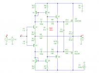
hec != hoax ?
Hi Pete,
In order to prove that HEC is equivalent to traditional NFB, I've simulated this simple output stage. It not only has the same performance in terms of distortion and stability, but the step response is much cleaner and there ain't no EC circuitry running out of steam under heavy loads. Furthermore, no large bias voltage (e.g 22V) is stolen from the VAS, so no need for a boosted power supply for the front end.
Some specs: THD20=50ppm at 100W into 8 Ohm, Iq = 150mA.
Cheers, Edmond.
PS: All PNPs are 2SA1407 and all NPNs are 2SC3601
PB2 said:
[snip]
Another challenge for the opposing view would be to show a simple traditional, local, negative feedback loop around the output stage that provides the same/similar performance. If it is all so simple, then show me an implementation, the solution is not obvious as it would be commonly used.
[snip]
Pete B.
Hi Pete,
In order to prove that HEC is equivalent to traditional NFB, I've simulated this simple output stage. It not only has the same performance in terms of distortion and stability, but the step response is much cleaner and there ain't no EC circuitry running out of steam under heavy loads. Furthermore, no large bias voltage (e.g 22V) is stolen from the VAS, so no need for a boosted power supply for the front end.
Some specs: THD20=50ppm at 100W into 8 Ohm, Iq = 150mA.
Cheers, Edmond.
PS: All PNPs are 2SA1407 and all NPNs are 2SC3601
Attachments
Hi Edmond
Hmmmm....... very pretty, but the -3dB bandwidth is only 2.6MHz (30 deg lag at 2MHz), so there is a greater limitation now on how much HF global NFB such an output stage can be wrapped up in???
Cheers,
Glen
Hmmmm....... very pretty, but the -3dB bandwidth is only 2.6MHz (30 deg lag at 2MHz), so there is a greater limitation now on how much HF global NFB such an output stage can be wrapped up in???
Cheers,
Glen
G.Kleinschmidt said:Hi Edmond
Hmmmm....... very pretty, but the -3dB bandwidth is only 2.6MHz (30 deg lag at 2MHz), so there is a greater limitation now on how much HF global NFB such an output stage can be wrapped up in???
Cheers,
Glen
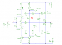
Hi Glen,
That's right, 2.6MHz. Fc is set rather conservatively. As for the 30 deg lag at 2MHz, if it's too much, you can reduce it to the same level as in HEC, i.e. 11deg, by moving the Miller compensation to the emitter of Q2 and Q3 respectively (see figure). However, this configuration gives a little bit of overshoot, although it is masked in a complete amp.
Cheers, Edmond.
Attachments

Re: hec != hoax
I'm not sure that you've proven it, however I do like your circuit and think it is good if my challenge was the push to produce this new topology. It is new I take it, I'm sure you or one of the brains here will correct me if not, LOL! You do in a sense have a VAS or gain stage in Q2, Q3, which is fine since HEC can be viewed as providing gain.
I see a similarity with the old Tiger output stage, perhaps simply with Q2-Q3 being CE and the local feedback. This circuit could provide some gain in order to reduce the swing requirement on the front end, so that it could be regulated, or use cascodes without the need for another supply.
I wonder if Bob might combine this with HEC, include some gain, and then not need the second supply for the front end. I've not looked close enough to determine if this is even possible, just throwing it out there.
I've been meaning to suggest the investigation of output stages with gain for some time now.
It seems that there's been some good discussion since my challenges, the thread moves fast and can be a large time sink so I've held off commenting. Jcx has done some nice work also:
http://www.diyaudio.com/forums/showthread.php?postid=1324657#post1324657
Still, it seems to me as others have commented, there is no reason that Bob could not add NDFL, or other techniques discussed to his design.
I agree with you and mentioned from the start that Bob's design is complex, however I do respect the fact that he had an ultra low distortion goal and used much older parts available at the time. I also do not like the requirement for boosted front end supplies. Just my preferences.
Pete B.
Edmond Stuart said:
Hi Pete,
In order to prove that HEC is equivalent to traditional NFB, I've simulated this simple output stage. It not only has the same performance in terms of distortion and stability, but the step response is much cleaner and there ain't no EC circuitry running out of steam under heavy loads. Furthermore, no large bias voltage (e.g 22V) is stolen from the VAS, so no need for a boosted power supply for the front end.
Some specs: THD20=50ppm at 100W into 8 Ohm, Iq = 150mA.
Cheers, Edmond.
PS: All PNPs are 2SA1407 and all NPNs are 2SC3601
I'm not sure that you've proven it, however I do like your circuit and think it is good if my challenge was the push to produce this new topology. It is new I take it, I'm sure you or one of the brains here will correct me if not, LOL! You do in a sense have a VAS or gain stage in Q2, Q3, which is fine since HEC can be viewed as providing gain.
I see a similarity with the old Tiger output stage, perhaps simply with Q2-Q3 being CE and the local feedback. This circuit could provide some gain in order to reduce the swing requirement on the front end, so that it could be regulated, or use cascodes without the need for another supply.
I wonder if Bob might combine this with HEC, include some gain, and then not need the second supply for the front end. I've not looked close enough to determine if this is even possible, just throwing it out there.
I've been meaning to suggest the investigation of output stages with gain for some time now.
It seems that there's been some good discussion since my challenges, the thread moves fast and can be a large time sink so I've held off commenting. Jcx has done some nice work also:
http://www.diyaudio.com/forums/showthread.php?postid=1324657#post1324657
Still, it seems to me as others have commented, there is no reason that Bob could not add NDFL, or other techniques discussed to his design.
I agree with you and mentioned from the start that Bob's design is complex, however I do respect the fact that he had an ultra low distortion goal and used much older parts available at the time. I also do not like the requirement for boosted front end supplies. Just my preferences.
Pete B.
Re: Re: hec != hoax
Hi Pete,
Thanks for your comments.
The "proof" is that, with the same amount of NFB and the same roll-off, the performance is also the same. OK, it's not a rock solid proof, so let's call it "strong evidence". 🙂
Whether it's new, I really don't know. Perhaps it is a re-invention, as happens to me so many times.
The VASes consists of Q5 and Q6 (not Q2 and Q3). As they are part of the current mirrors, the current gain is of course rather low, in fact unity.
I had a quick look at the Tiger OPS, but I don't think there are many similarities, as it asymmetric and the output trannies are put in a CE configuration for example.
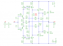
As for some gain, yes, it's possible. Put a 1kOhm resistor between node A and ground.
I've dropped here another version with Schottky diodes, which also eliminates the overshoot. Also the quiescent of the input stage and current mirrors has been lowered, so that cheaper trannies can be used.
BTW, the slew rate is 1GV/s 😀
Cheers, Edmond.
PB2 said:I'm not sure that you've proven it, however I do like your circuit and think it is good if my challenge was the push to produce this new topology. It is new I take it, I'm sure you or one of the brains here will correct me if not, LOL! You do in a sense have a VAS or gain stage in Q2, Q3, which is fine since HEC can be viewed as providing gain.
I see a similarity with the old Tiger output stage, perhaps simply with Q2-Q3 being CE and the local feedback. This circuit could provide some gain in order to reduce the swing requirement on the front end, so that it could be regulated, or use cascodes without the need for another supply.
I wonder if Bob might combine this with HEC, include some gain, and then not need the second supply for the front end. I've not looked close enough to determine if this is even possible, just throwing it out there.
I've been meaning to suggest the investigation of output stages with gain for some time now.
It seems that there's been some good discussion since my challenges, the thread moves fast and can be a large time sink so I've held off commenting. Jcx has done some nice work also:
http://www.diyaudio.com/forums/showthread.php?postid=1324657#post1324657
Still, it seems to me as others have commented, there is no reason that Bob could not add NDFL, or other techniques discussed to his design.
I agree with you and mentioned from the start that Bob's design is complex, however I do respect the fact that he had an ultra low distortion goal and used much older parts available at the time. I also do not like the requirement for boosted front end supplies. Just my preferences.
Pete B.
Hi Pete,
Thanks for your comments.
The "proof" is that, with the same amount of NFB and the same roll-off, the performance is also the same. OK, it's not a rock solid proof, so let's call it "strong evidence". 🙂
Whether it's new, I really don't know. Perhaps it is a re-invention, as happens to me so many times.
The VASes consists of Q5 and Q6 (not Q2 and Q3). As they are part of the current mirrors, the current gain is of course rather low, in fact unity.
I had a quick look at the Tiger OPS, but I don't think there are many similarities, as it asymmetric and the output trannies are put in a CE configuration for example.
As for some gain, yes, it's possible. Put a 1kOhm resistor between node A and ground.
I've dropped here another version with Schottky diodes, which also eliminates the overshoot. Also the quiescent of the input stage and current mirrors has been lowered, so that cheaper trannies can be used.
BTW, the slew rate is 1GV/s 😀
Cheers, Edmond.
Attachments
Re: hec != hoax ?
Hi Edmond,
Nice work. I always like it when someone shows that there is more than one way to skin a cat.
Why didn't you use this circuit in your PGP instead of EC? 🙂. I assume you came up with this afterwards.
I do have to take issue with a couple of things you said about EC.
The EC circuit does not run out of steam under heavy loads. Just look at my Figure 20 in my MOSFET amplifier paper, where I drove over 22 Amps into a 1 ohm load at 20 kHz with a 2-cycle burst, using only a single pair of output devices.
I do recall that you showed a simulation of that where the error difference transistors were clipping, but in that simulation you were taking liberties with the design and using faulty MOSFET models. You added 0.22 ohm source resistors without accounting for their 4V drop at 20 amps. You also used an IRFP244 with a wimpy model that only put out 8.8 amps with a forward gate voltage of 7V. The IRFP240 data sheet shows 21 Amps at 7V.
The original EC circuit was designed to put out between 8 and 9V of turn-on voltage with respect to the output rail. As long as that capability is properly matched with the output devices, the EC circuit will not run out of steam.
In your circuit you are also taking advantage of the lower turn-on voltage of the Toshiba MOSFETs.
In more recent designs I use folded emitter followers to drive the EC, with the voltage spreading taking place after the folded EF, so the bias voltage is not stolen from the VAS. Moreover, no matter what you do, you need to have enough drive voltage ultimately to adequately forward bias the output MOSFETs. If you choose not to use a boosted supply anywhere, you are certainly free to do so, but you may be putting an unnecessarily large main high current power supply voltage on the output devices, dissipating more than need be. If one wishes to make such a compromise, it can be done with EC as well.
Nevertheless, your interesting design is about efficeint as one can get as long as you don't want to be able to swing the gate beyond the supply voltage. The use of the Toshibas makes this less of an issue anyway.
I generally like boosted supplies, and if you use one, a difference of a couple of volts one way or the other is no big deal. The boosted supplies are relatively inexpensive due to the low current needs, and the bit of extra headroom they give the VAS can help performance. Just a matter of choice. But in a truly high-performance amplifier a boosted supply is no big deal.
Cheers,
Bob
Edmond Stuart said:
Hi Pete,
In order to prove that HEC is equivalent to traditional NFB, I've simulated this simple output stage. It not only has the same performance in terms of distortion and stability, but the step response is much cleaner and there ain't no EC circuitry running out of steam under heavy loads. Furthermore, no large bias voltage (e.g 22V) is stolen from the VAS, so no need for a boosted power supply for the front end.
Some specs: THD20=50ppm at 100W into 8 Ohm, Iq = 150mA.
Cheers, Edmond.
PS: All PNPs are 2SA1407 and all NPNs are 2SC3601
Hi Edmond,
Nice work. I always like it when someone shows that there is more than one way to skin a cat.
Why didn't you use this circuit in your PGP instead of EC? 🙂. I assume you came up with this afterwards.
I do have to take issue with a couple of things you said about EC.
The EC circuit does not run out of steam under heavy loads. Just look at my Figure 20 in my MOSFET amplifier paper, where I drove over 22 Amps into a 1 ohm load at 20 kHz with a 2-cycle burst, using only a single pair of output devices.
I do recall that you showed a simulation of that where the error difference transistors were clipping, but in that simulation you were taking liberties with the design and using faulty MOSFET models. You added 0.22 ohm source resistors without accounting for their 4V drop at 20 amps. You also used an IRFP244 with a wimpy model that only put out 8.8 amps with a forward gate voltage of 7V. The IRFP240 data sheet shows 21 Amps at 7V.
The original EC circuit was designed to put out between 8 and 9V of turn-on voltage with respect to the output rail. As long as that capability is properly matched with the output devices, the EC circuit will not run out of steam.
In your circuit you are also taking advantage of the lower turn-on voltage of the Toshiba MOSFETs.
In more recent designs I use folded emitter followers to drive the EC, with the voltage spreading taking place after the folded EF, so the bias voltage is not stolen from the VAS. Moreover, no matter what you do, you need to have enough drive voltage ultimately to adequately forward bias the output MOSFETs. If you choose not to use a boosted supply anywhere, you are certainly free to do so, but you may be putting an unnecessarily large main high current power supply voltage on the output devices, dissipating more than need be. If one wishes to make such a compromise, it can be done with EC as well.
Nevertheless, your interesting design is about efficeint as one can get as long as you don't want to be able to swing the gate beyond the supply voltage. The use of the Toshibas makes this less of an issue anyway.
I generally like boosted supplies, and if you use one, a difference of a couple of volts one way or the other is no big deal. The boosted supplies are relatively inexpensive due to the low current needs, and the bit of extra headroom they give the VAS can help performance. Just a matter of choice. But in a truly high-performance amplifier a boosted supply is no big deal.
Cheers,
Bob
Edmond,
This isn't a new topology but it is an effective alternative way to apply NFB to the FETs using 8 transistors. There are pros and cons. I agree with your hypothesis that similar performance is caused by similar NFB; implying HEC is not doing any error cancelling or other hocus pocus.
Brian
This isn't a new topology but it is an effective alternative way to apply NFB to the FETs using 8 transistors. There are pros and cons. I agree with your hypothesis that similar performance is caused by similar NFB; implying HEC is not doing any error cancelling or other hocus pocus.
Brian
Edmond Stuart said:
Hi Glen,
That's right, 2.6MHz. Fc is set rather conservatively. As for the 30 deg lag at 2MHz, if it's too much, you can reduce it to the same level as in HEC, i.e. 11deg, by moving the Miller compensation to the emitter of Q2 and Q3 respectively (see figure). However, this configuration gives a little bit of overshoot, although it is masked in a complete amp.
Cheers, Edmond.
😎
That miller comp mod will give you a better PSRR too. But don't be too complacent about a little bit of overshoot in the OPS.
It may be masked by the closed loop gain in a complete amp, but the open loop gain is effected and the amplifier can have a reduced gain margin at the frequency peak, causing conditional stablilty issues (especially bursts of oscillation of the leading edges when going in and out of clipping.
Cheers,
Glen
- Home
- Amplifiers
- Solid State
- Bob Cordell Interview: Error Correction