darkfenriz said:
One more thing R21, R23 & R25 are on the wrong side of the FET. With the resistors on the source the current sharing works better because as current increase through one FET the voltage drop across the source resistor increases. This means that the gate to source voltage is reduced and the FET backs off.
This is a common mistake with quasi-complimentary amps and this part of the topology is often confused with NPN/PNP output stages.
Cheers
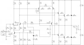
High Power Version;
This is the same amp modified to handle much higher rails.
By using the seperate 100v feed on the positive side of the input and driver stage the amp can swing the output closer to the positive rail and provide more power.
The main difference is the addition of a cascode arrangement in the driver stage using P channel FETs.
With the right power supply this amp should be able to deliver around 350 watts into 8 ohms and around 650 into 4 ohms.
This design is intended as a PA amplifier driving big speakers.
Cheers
Attachments
quasi said:One more thing R21, R23 & R25 are on the wrong side of the FET. With the resistors on the source the current sharing works better because as current increase through one FET the voltage drop across the source resistor increases. This means that the gate to source voltage is reduced and the FET backs off.
This is a common mistake with quasi-complimentary amps and this part of the topology is often confused with NPN/PNP output stages.
Cheers
This is not strictly true, either way can work. The reason that it works if you use what appears to be drain resistor is because of the local feedback wrapped around the output device. Peter Baxandall wrote a letter in Wireless World in September 1969 describing the operation.
However, I believe that in case of the schematic posted you are correct as the local feedback does not take place in the same way and thus the resistors should be in the sources.
Interesting
I wonder why they use such a complicated thermal compensation circuit. Well I better build my version then and find out.
I still think that the negative rail output FETs are on the wrong side i.e. they should be on the source. It does make the short cct protection slightly easier to configure though.
Looks like they are only running around 4 mA of driver current per leg.
Cheers
edl said:
I wonder why they use such a complicated thermal compensation circuit. Well I better build my version then and find out.
I still think that the negative rail output FETs are on the wrong side i.e. they should be on the source. It does make the short cct protection slightly easier to configure though.
Looks like they are only running around 4 mA of driver current per leg.
Cheers
traderbam said:Hi Quasi,
Interesting design. I understand you haven't built it yet. Have you simulated it?
My question is about the stability of the feedback loop...have you estimated/simulated the phase margin?
BAM
No I haven't built it yet or simulated it (I don't have sim software). I'll build one over the next week or so. I'll probably just build one to test it and then use it as a sub-amp or something...hmm.
The feedback loop is one I have always used (and almost everyone else too). I see no reason for it not to be stable.
Anyway I'll update in a week or so.
Cheers
Re: Re: confusion
Hi buddy,
The voltage will be clamped with respect to VGS in positive direction and the diode in series only exhibits forward drop.
I see no reason for its place.
In negative direction[without the diode]the voltage will be clamped to forward drop of zener itself.
kindly correct me if am wrong,
regards,
kanwar
richie00boy said:quasi,
Thanks for the complimentYou do not need to include a normal diode in the lower zener diode because there is absolutely no risk of current reaching up through it.
Hi Kanwar,
No, you must include the diode. As you say the voltage will be clamped at 12V, but surely it's far better to stop the spurious transients even being a problem. They will cause distortion.
Hi buddy,
The voltage will be clamped with respect to VGS in positive direction and the diode in series only exhibits forward drop.
I see no reason for its place.
In negative direction[without the diode]the voltage will be clamped to forward drop of zener itself.
kindly correct me if am wrong,
regards,
kanwar
You are right. I'm just saying that the diode prevents even having to even clamp any voltage in the negative direction. If any voltage gets up to the gate it will cause distortion. The gate will not be destroyed without the diode, I'm just recommending it to obtain minimum distortion.
Q6
Hmm...Q6 seems to share the rail to rail voltage with Q5 in a cascode arrangement. This keeps both transistors operating within their SOAR.
In my cct because I use MJE350's the cascode is not necessary because even with approximately 100v across my T6 (atrk n-mos 1v2.pdf) and with 18mA it is still well within its SOAR.
Thanks for the cct & Cheers
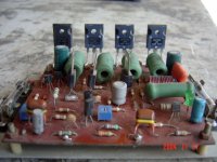
Propsed Layout - low power version;
This is the proposed layout for the lower power version. Depending on the FET's and power supply used, this board could deliver around 200 watts into 4 ohms maybe more.
I'll build one over the next week or so.
Cheers
This is the proposed layout for the lower power version. Depending on the FET's and power supply used, this board could deliver around 200 watts into 4 ohms maybe more.
I'll build one over the next week or so.
Cheers
Attachments
Re: Propsed Layout - low power version;
good luck, Dear Quasi!
I'm really courious, how will the amp sounds, and how will the measurements looking like!
In the summer I'm going to bulid a quasi-complementary mosfet design for almost +/-100V rails, with a lot of IRFP240's.
Please write to this topic, as soon as the amp works!
Hello from Hungary!
(sorry for my bad english... )
quasi said:This is the proposed layout for the lower power version. Depending on the FET's and power supply used, this board could deliver around 200 watts into 4 ohms maybe more.
I'll build one over the next week or so.
Cheers
good luck, Dear Quasi!
I'm really courious, how will the amp sounds, and how will the measurements looking like!
In the summer I'm going to bulid a quasi-complementary mosfet design for almost +/-100V rails, with a lot of IRFP240's.
Please write to this topic, as soon as the amp works!
Hello from Hungary!
(sorry for my bad english...
)B.I.G said:could you post the bottom layout ?
Following are pdf's containing the copper side and latest schematic of the low power version.
Note that the BC546's used as T1 & T3 are only suitable for the rail voltages shown and even then they are right on the limit. If higher rails are used then a different transistor must be used. 2SC1845 is very nice but it has different pinouts.
If you build this amp please let me know the results.
Cheers
Attachments
I didn't want to start a new tread because my subject is related to this tread.
I like the quasi-complementary design because I think easier to find transistors with similar parameters of the same type than of complementar pairs.
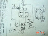
Lately I have found an interesting Russian page George Krilov - http://geocities.com/researchtriangle/node/2356/
http://geocities.com/researchtriangle/node/2356/newscheme.html - On this site the last schematic is a quasi-complementer design
The schematic uses bipolar transistors and the author wrote that the circuit is not stable yet, but he gives some advice as to how to correct it.
What do you think about the schematic?
I like the quasi-complementary design because I think easier to find transistors with similar parameters of the same type than of complementar pairs.
Lately I have found an interesting Russian page George Krilov - http://geocities.com/researchtriangle/node/2356/
http://geocities.com/researchtriangle/node/2356/newscheme.html - On this site the last schematic is a quasi-complementer design
The schematic uses bipolar transistors and the author wrote that the circuit is not stable yet, but he gives some advice as to how to correct it.
What do you think about the schematic?
- Status
- This old topic is closed. If you want to reopen this topic, contact a moderator using the "Report Post" button.
- Home
- Amplifiers
- Solid State
- Another quasi-complementary design