Hello Tibi,
You will have to run the KICAD DRC. You have unconnected tracks and "clearance" problems in the PCB.
Cheers,
Stef.
You will have to run the KICAD DRC. You have unconnected tracks and "clearance" problems in the PCB.
Cheers,
Stef.
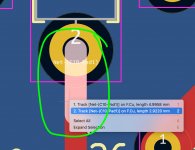
Thank you, Stef. Yes, I run DRC. Clearance errors are mainly due part numbering and others are related to castellated holes.
Regards,
Tibi
Regards,
Tibi
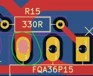
Hi Tibi,
I was thinking for example of this type of error. Unconnected tracks that drag below the others. Pieces of track that are no longer useless.
Uploaded v1.0.3 of the mini PCB. Changed some footprints for small signal transistors, moved some tracks and added one hole at 10mm for C17. More parts will be usable there.
Github
Stef.
** Found 460 DRC violations **
[via_dangling]: Via is not connected or connected on only one layer
Local override; Severity: warning
@(191.5400 mm, 95.3600 mm): Via [<no net>] on F.Cu - B.Cu
[via_dangling]: Via is not connected or connected on only one layer
Local override; Severity: warning
@(190.8400 mm, 96.0600 mm): Via [<no net>] on F.Cu - B.Cu
[via_dangling]: Via is not connected or connected on only one layer
Local override; Severity: warning
@(192.2400 mm, 96.0600 mm): Via [<no net>] on F.Cu - B.Cu
[via_dangling]: Via is not connected or connected on only one layer
Local override; Severity: warning
@(191.5400 mm, 96.7600 mm): Via [<no net>] on F.Cu - B.Cu
[track_dangling]: Track has unconnected end
Local override; Severity: warning
.
Attachments
Last edited:
Got the boards.
Gerbers on these pcb can be found or are there not free to access?
Thanks.

So I can now write something about the second setup with 3 pairs of end transistors:
First the totally frustrating thing: The bass becomes more undefined and the treble is no longer so ultra clean and atmospheric.
About the construction:
I built the new boards very carefully, measured the components and selected for tight tolerances through the mountains of components I now have.
Then I put the amplifier into operation and the additional noise was much louder than with my first version. It rattled, like a very old amplifier.
Then came the analysis as to why:
Well I left a lot of nerves, but by arguments of atiq19 prophylactically added the C-Q5 and C-Q6 to the new layout. With 2.2nF the complete spook (additional noise, something like IMD) is gone.
Now to my thesis:
I measured the Mosfet in cold condition and installed them in groups of three with small tolerances. In this power spectrum, they played well in both the first and the second layout - i.e. in the mW range, very quietly.
Now the first layout had large trace areas that logically behave as capacitors, plus there were the very small capacitors for C7 from an MKP2 and an FKP2 from Wima. Therefore, I assume that both effects had a favourable effect on the additional noise and that the distortions were therefore quieter than with the current layout.
With the new layout, I specially replaced the trace areas with double-sided traces to eliminate these effects. Then I increased R23 to the 10k given by Tibi and I tried out how the additional capacitors (C-Q5 and C-Q6) with 2.2nF (Styroflex, like C1 and C10) affect the level, which, according to the simulation, clearly reduce the level in the MHz range, but show no effects in the audible spectrum up to about 100kHz. These capacitors make the amplifier play clean.
But, it is too sharp in the highs. I already had this sharpness with my test setup with two pairs of end transistors. Therefore, I have now installed 1uF Wima MKP10 1600V as C7. These capacitors play nice voices and the highs are less harsh.
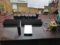
The amplifier now runs with the three pairs of end transistors, +- 53V and active rectification. This amplifier has 6.9mF installed on each board for voltage stabilisation and 4.7mF at the rectifier.
The old amplifier runs with a pair of end transistors, +- 36V and normal rectifier diodes. This amplifier has only 0.47 mF on the board and 20 mF at the rectifier for both channels.
It feels like the old amplifier plays even lower, because it can also convey the noises from the stage very cleanly, the touches simply sound more controlled. There is little difference in the three-dimensionality of the two amplifiers, but the new one lacks airiness. This is something that has already been mentioned here, which is typical for the parallel power amplifier. Of course, I didn't expect the new amplifier to lose that much.
It is now of course exciting to see how the others get their amplifiers to play.I'm curious about Vrystaat, he should be ready and able to test soon. I hope for success reports.
First the totally frustrating thing: The bass becomes more undefined and the treble is no longer so ultra clean and atmospheric.
About the construction:
I built the new boards very carefully, measured the components and selected for tight tolerances through the mountains of components I now have.
Then I put the amplifier into operation and the additional noise was much louder than with my first version. It rattled, like a very old amplifier.
Then came the analysis as to why:
Well I left a lot of nerves, but by arguments of atiq19 prophylactically added the C-Q5 and C-Q6 to the new layout. With 2.2nF the complete spook (additional noise, something like IMD) is gone.
Now to my thesis:
I measured the Mosfet in cold condition and installed them in groups of three with small tolerances. In this power spectrum, they played well in both the first and the second layout - i.e. in the mW range, very quietly.
Now the first layout had large trace areas that logically behave as capacitors, plus there were the very small capacitors for C7 from an MKP2 and an FKP2 from Wima. Therefore, I assume that both effects had a favourable effect on the additional noise and that the distortions were therefore quieter than with the current layout.
With the new layout, I specially replaced the trace areas with double-sided traces to eliminate these effects. Then I increased R23 to the 10k given by Tibi and I tried out how the additional capacitors (C-Q5 and C-Q6) with 2.2nF (Styroflex, like C1 and C10) affect the level, which, according to the simulation, clearly reduce the level in the MHz range, but show no effects in the audible spectrum up to about 100kHz. These capacitors make the amplifier play clean.
But, it is too sharp in the highs. I already had this sharpness with my test setup with two pairs of end transistors. Therefore, I have now installed 1uF Wima MKP10 1600V as C7. These capacitors play nice voices and the highs are less harsh.
The amplifier now runs with the three pairs of end transistors, +- 53V and active rectification. This amplifier has 6.9mF installed on each board for voltage stabilisation and 4.7mF at the rectifier.
The old amplifier runs with a pair of end transistors, +- 36V and normal rectifier diodes. This amplifier has only 0.47 mF on the board and 20 mF at the rectifier for both channels.
It feels like the old amplifier plays even lower, because it can also convey the noises from the stage very cleanly, the touches simply sound more controlled. There is little difference in the three-dimensionality of the two amplifiers, but the new one lacks airiness. This is something that has already been mentioned here, which is typical for the parallel power amplifier. Of course, I didn't expect the new amplifier to lose that much.
It is now of course exciting to see how the others get their amplifiers to play.I'm curious about Vrystaat, he should be ready and able to test soon. I hope for success reports.
Last edited:
Tibi,
I got a box full of them, new old stuff and I have used them plenty of times before, I reform them for 24 hours with current limiting resistors en then 80% of rated voltage. They test very good.
Tim, there will be others before me, this time I take my time and enjoy the build, still have to make boards for softstart and speaker protection.I'm in no hurry ! lol
What is happening with Alex's builds and the other guy's, will be great to get some feedback !
Hi Tibi,
I was thinking for example of this type of error. Unconnected tracks that drag below the others. Pieces of track that are no longer useless.
...
Thank you Stef for this observation.
I spent yesterday several hours to clear a ton of errors.
Now things look far better -> github
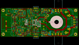
Next step is to add one more pair and move final pairs at the edge of the board with castellated holes.
Regards,
Tibi
...
Then came the analysis as to why:
Well I left a lot of nerves, but by arguments of atiq19 prophylactically added the C-Q5 and C-Q6 to the new layout. With 2.2nF the complete spook (additional noise, something like IMD) is gone.
...
Thank you very much for your feedback !
I suppose you have added these capacitors between gate and drain. If this is the case, than 2,2nF it is too large. A more appropriate value would be in range of 100pF and 330pF.
Have you used any balast resistor at output stage ? Matching 3 mosfets it far too hard than two. A 0.1ohm resistor in source of each will do the trick.
Oscillation may occur when high gain input stage, opamp and cascode, is close to current dumping bridge. Keep these parts away 20-30-mm from each other and amplifier will be stable.
Regads,
Tibi
I measured the Mosfet in cold condition
Hello Tim,
I may make a mistake but for me, the power MOSFETs must be measured when hot once stabilized and at a voltage close to that of the circuit. This is the method I followed when I built a Pass Aleph.
Cheers,
Stef.
https://www.firstwatt.com/pdf/art_matching.pdf
Amplificateur Aleph
.
Thank you very much for your feedback !
I suppose you have added these capacitors between gate and drain. If this is the case, than 2,2nF it is too large. A more appropriate value would be in range of 100pF and 330pF.
Have you used any balast resistor at output stage ? Matching 3 mosfets it far too hard than two. A 0.1ohm resistor in source of each will do the trick.
Oscillation may occur when high gain input stage, opamp and cascode, is close to current dumping bridge. Keep these parts away 20-30-mm from each other and amplifier will be stable.
Regads,
Tibi
Hello Tibi,
do you mean the spatial separation of Q7 - R5 - Q8 from the components: C10 + R26, R27, R28 + L1?
That is only a few mm apart on my layout. There should be a larger distance where the blue line runs?
On my old layout, Q7 is further away and sits further forward.
Attachments
Hello Tim,
I may make a mistake but for me, the power MOSFETs must be measured when hot once stabilized and at a voltage close to that of the circuit. This is the method I followed when I built a Pass Aleph.
Cheers,
Stef.
That is absolutely correct, I have so far also achieved very good results only by selection with a component tester, there was so far no requirement to select warm components under load.
But the level of the Q17 is extremely high. The new Q17 also performs outstandingly - just not in direct comparison with the older model.
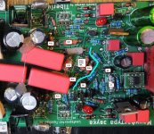
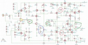
here is a picture of the construction and the circuit diagram(green=filter in the original, blue=filter against oscillation of my old setup, green=additional filters of the current setup).
I increased the resistance of the source to 0.15 (measured approx. 140mOhm). I measure the air coil with approx. 20mOhm.
I increased the resistance of the source to 0.15 (measured approx. 140mOhm). I measure the air coil with approx. 20mOhm.
Attachments
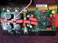
sorry for a typo in my post above, the additional capacitors that I only activated on the current model are the ones circled in red.
Thank you very much for your feedback !
I suppose you have added these capacitors between gate and drain. If this is the case, than 2,2nF it is too large. A more appropriate value would be in range of 100pF and 330pF.
I used LTspice to analyse the effect of C-Q5 and C-Q6. The picture that results from the original circuit is that a resonance happens at 5.7MHz (middle picture), which can be smoothed by 330pF (upper picture) and the built-in 2.2nF (lower picture) doesn't really change anything significantly. 100pF is too small according to the simulation. The real errors of the components certainly lead to a lower resonance frequency, which of course means that with the 2.2nF everything can be smoothed. According to the simulation, a value in the range of 330pF to 470pF should be sufficient for the oscillation damping.
Attachments

Hello Tim,
I may make a mistake but for me, the power MOSFETs must be measured when hot once stabilized and at a voltage close to that of the circuit. This is the method I followed when I built a Pass Aleph.
...
Pass Aleph is a class A amplifier and output mosfets will operate hot.
Q17 is class B amplifier and output transistors are cold. In this case what mattes is Vgs at room temperature and if you want to pair them, this must be done at room temperature. As soon they start to operate, Vgs will start to drop.
Regads,
Tibi
Hello Tibi,
do you mean the spatial separation of Q7 - R5 - Q8 from the components: C10 + R26, R27, R28 + L1?
That is only a few mm apart on my layout. There should be a larger distance where the blue line runs?
On my old layout, Q7 is further away and sits further forward.
Seems these are not so close, but I must admit is hard to follow your layout. 😀
Please make sure opamp is decoupled with two 100nF as close as possible.
As a general design rule, current dumping bridge must be kept away from cascode stage. Inductor as isolated as possible.
Regards,
Tibi
Attachments
I used LTspice to analyse the effect of C-Q5 and C-Q6. The picture that results from the original circuit is that a resonance happens at 5.7MHz (middle picture), which can be smoothed by 330pF (upper picture) and the built-in 2.2nF (lower picture) doesn't really change anything significantly. 100pF is too small according to the simulation. The real errors of the components certainly lead to a lower resonance frequency, which of course means that with the 2.2nF everything can be smoothed. According to the simulation, a value in the range of 330pF to 470pF should be sufficient for the oscillation damping.
Here are my comments on your schematic:
1. pcb layout is important and can make big difference in amplifier operation
2. C1 will limit amplifier bw. You may increase this up 1nF
3. in your schematic C-Q5 and C-Q6 should be moved to Q5 and Q6 between gate and drain. Use silver-mica or polystyrene for best results. Start with 100pF.
4. don't touch C10 unless you change other parts in current dumping bridge
5. adding R22 and C27 will add another pole and because is in negative reaction, over R6 and will increase amplifier gain at high frequency making things even unstable.
And here are general my suggestions to improve amplifier stability, for those will approach this construction:
1. keep current dumping bridge away from opamp and cascode stage.
2. Increase R5 up to 100ohm
3. add an capacitor 100pF between gate and drain on Q5 (silver-mica or polystyrene)
4. In case you mave multiple output pairs, increase class A current stage by lowering R10 & R13. I would say 100mA is enough to drive any mosfet. In this case R10=R13=6ohm.
5. In case you use very high speed output mosfets, like Exicon laterals, increase gate resistors from 330ohm to 660ohm or higher. Take care that N and P laterals have different input capacitance . For example: Ciss for ECW20N20 is 900pF and Ciss for ECW20P20 is 1800pF. This would translate in gate resistor for N=660ohm and P = 1k2.
Regards,
Tibi
Last edited by a moderator:
- Home
- Amplifiers
- Solid State
- Q17 - an audiophile approach to perfect sound