Dear audio enthusiasts on DIY Audio,
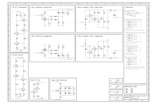
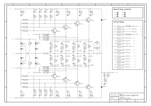
I plan to build an amplifier front end that is heavily based on Bob Cordell's CordellAudio.com - A MOSFET Power Amplifier with Error Correction amplifier from 1984.
I also implemented some ideas from his excellent book and some further ideas collected or developed over some years.
The design looks pretty complex, but most of the complexity is not in the signal chain.
Some design goals:
The design looks totally over-engineered, but I had something in mind with every complication I added.
I present the design here because I like to hear the experts opinion, kind of peer review.
I gain a lot of inspiration on the forum and like to share what I do in order to maybe inspire other DIYers.
I'm not really interested in simplification of the design unless this would improve performance.
Some design justification:
The CCS are so huge because their output current does not vary at all with supply voltage. Also the PSRR is impressive. They are pretty stable.
The VAS has its own CCS, which is not really necessary, but allows setting standing current of first and second LTP independently. Can be omitted easily in case this is not desired.
The input over-voltage protection aims to protect the sensitive transistors from ESD and other high voltage events for both inputs. The design is simple, effective, does not worsen distortion significantly and is optional to assemble. I just find that inputs deserve protections since exceeding the absolute maximum rating of the input transistors voltage will degrade or destroy them. The standard low pass filter does a lot to mitigate ESD already and the additional protection is just for more severe cases.
Capacitance multipliers are great. This is Keantoken's design. Thanks a lot!
The rail reference sense makes sure that the output stage cannot be driven into saturation. Zener diodes values need to be adjusted to the type of output transistor used (BJT, vertical MOSFET or lateral MOSFET).
I use CFPs in the first LTP. While this does not show any improvement in simulation, I still like to try this. In any case, it makes this stage more linear. I stumbled across an article, that this helps to minimize memory distortion. So maybe worth a try. In case it doesn't work well, it can be reverted to the classic design easily.
I'm looking forward to your comments.
Easter is coming. And every project needs a name. So this is the Bunnyphant.
Best regards,
Lee
I plan to build an amplifier front end that is heavily based on Bob Cordell's CordellAudio.com - A MOSFET Power Amplifier with Error Correction amplifier from 1984.
I also implemented some ideas from his excellent book and some further ideas collected or developed over some years.
The design looks pretty complex, but most of the complexity is not in the signal chain.
Some design goals:
- High PSRR
- Power supply invariant operation
- Massive input over-voltage protection
- Feedback Baker clamps to maintain NFB during clipping
- Adaptive clipping by sensing output stage voltage
The design looks totally over-engineered, but I had something in mind with every complication I added.
I present the design here because I like to hear the experts opinion, kind of peer review.
I gain a lot of inspiration on the forum and like to share what I do in order to maybe inspire other DIYers.
I'm not really interested in simplification of the design unless this would improve performance.
Some design justification:
The CCS are so huge because their output current does not vary at all with supply voltage. Also the PSRR is impressive. They are pretty stable.
The VAS has its own CCS, which is not really necessary, but allows setting standing current of first and second LTP independently. Can be omitted easily in case this is not desired.
The input over-voltage protection aims to protect the sensitive transistors from ESD and other high voltage events for both inputs. The design is simple, effective, does not worsen distortion significantly and is optional to assemble. I just find that inputs deserve protections since exceeding the absolute maximum rating of the input transistors voltage will degrade or destroy them. The standard low pass filter does a lot to mitigate ESD already and the additional protection is just for more severe cases.
Capacitance multipliers are great. This is Keantoken's design. Thanks a lot!
The rail reference sense makes sure that the output stage cannot be driven into saturation. Zener diodes values need to be adjusted to the type of output transistor used (BJT, vertical MOSFET or lateral MOSFET).
I use CFPs in the first LTP. While this does not show any improvement in simulation, I still like to try this. In any case, it makes this stage more linear. I stumbled across an article, that this helps to minimize memory distortion. So maybe worth a try. In case it doesn't work well, it can be reverted to the classic design easily.
I'm looking forward to your comments.
Easter is coming. And every project needs a name. So this is the Bunnyphant.
Best regards,
Lee
Attachments

I have used the circuit given for the tail and reference ccs in multiple designs spanning 20yrs without a startup resistor and it has never failed to start. I even stuck one in the deep freeze for a few hours and it started no problem. In theory the circuit might fail to start but in practice, never!
Whether or not the CSS startup is a likely issue, I prefer to be on the safe side and adding three cheap resistors in the first place is better than maybe having a problem later.
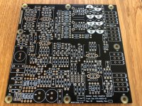
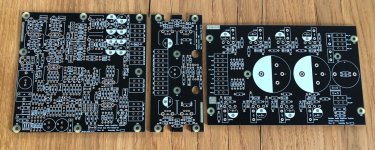
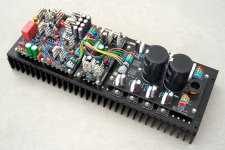
PCBs arrived and I'm looking forward to assembly. This may take quite some time.
This front end is part of my modular amplifier system and the first pairing will be with a folded driver and an output stage that has four pairs of BJT.
PCBs arrived and I'm looking forward to assembly. This may take quite some time.
This front end is part of my modular amplifier system and the first pairing will be with a folded driver and an output stage that has four pairs of BJT.
Attachments
Making a LTP from CFPs works well.
It linearises the varying gm of the two active devices, so that the horizontal S curve of the LTP is flattened. The linearity of LTPs is worst at high amplitude, particularly like bass signals. I used this concept in a series of kit amps from 2007 called the Lifeforce, and it worked very well, giving the amp very good bass response and great resolution.
Great thinking, like your amp!
HD
in this case this URL under
Memory Distortion Philosophies
and this threads also of interest:
cancelling memory distortion ?
Lavaradin Amp and "Memory distortion"...
Memory distortion, crap or serious?
Memory Distortion Philosophies
and this threads also of interest:
cancelling memory distortion ?
Lavaradin Amp and "Memory distortion"...
Memory distortion, crap or serious?
Hugh, thank you very much for confirming that CFPs inside LTPs are a good idea.
I had some linearisation in mind and you explained the effect very well so I now better understand why I did it this way.
Thanks for the compliment! Coming from you, that means a lot to me.
Tiefbassuebertr, thank you very much for the links.
I came across Peufeu's work doing research regarding the CFPs. Apart from Douglas Self, who mentioned CFP LTPs in his book, this was the only reference to a working design that I found.
Actually, combating memory distortion was not the primary goal, but having something special in a design is always good as it adds some mystery to the design and a flair of specialty.
Meanwhile I built the front end and also the folded driver and output stage module. Below image shows the Bunnyphant together with her companions mounted to the radiator.
I haven't had any time to really test this example amplifier configuration.
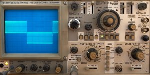
What I can say for now is that the front end DC conditions are as expected and it produces razor sharp square waves with negative feedback taken from the front end output.
I had some linearisation in mind and you explained the effect very well so I now better understand why I did it this way.
Thanks for the compliment! Coming from you, that means a lot to me.
Tiefbassuebertr, thank you very much for the links.
I came across Peufeu's work doing research regarding the CFPs. Apart from Douglas Self, who mentioned CFP LTPs in his book, this was the only reference to a working design that I found.
Actually, combating memory distortion was not the primary goal, but having something special in a design is always good as it adds some mystery to the design and a flair of specialty.
Meanwhile I built the front end and also the folded driver and output stage module. Below image shows the Bunnyphant together with her companions mounted to the radiator.
I haven't had any time to really test this example amplifier configuration.
What I can say for now is that the front end DC conditions are as expected and it produces razor sharp square waves with negative feedback taken from the front end output.
Attachments
I started electrical evaluation and while the first results were promising, I soon stumbled into problems:
The front end shows nice square wave response either open loop or with the loop closed right after its output.
Also, the driver stage and output stage seem to work fine, at least with the very small square wave signal I have available for feeding into the modules (oscilloscope test signal).
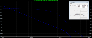
However, as soon as I connect the front end to the driver (and output stage), there is a sustained 250kHz oscillation. This is regardless whether there is any input signal or whether I close the feedback loop right after the front end or after the output stage. Connecting the modules together is enough to cause this weird oscillation, that is also pretty high in amplitude.
The 250kHz oscillation is superimposed on everything - no input, square or sine wave - it is always there.
I tried a massive shunt capacitor parallel to C83 at the output of the front end. 1nF causes the oscillation to decay within 150us after the slope of the square wave and 2n2 cures the oscillation, but this brute force approach totally destroys gain and phase of the amplifier.
According to simulation, the complete amplifier should have enough gain and phase margin (could me more though).
Has anybody seen such weird effects before?
I have no idea what could be going on here.
It must be so big that I cannot see it.
I find the frequency is way too low for parasitic oscillation. This should be in the 10s or 100s of MHz somewhere, not a few 100kHz.
I tried identifying something that could explain the long time constant, but didn't see anything.
Any help is highly appreciated!
The front end shows nice square wave response either open loop or with the loop closed right after its output.
Also, the driver stage and output stage seem to work fine, at least with the very small square wave signal I have available for feeding into the modules (oscilloscope test signal).
However, as soon as I connect the front end to the driver (and output stage), there is a sustained 250kHz oscillation. This is regardless whether there is any input signal or whether I close the feedback loop right after the front end or after the output stage. Connecting the modules together is enough to cause this weird oscillation, that is also pretty high in amplitude.
The 250kHz oscillation is superimposed on everything - no input, square or sine wave - it is always there.
I tried a massive shunt capacitor parallel to C83 at the output of the front end. 1nF causes the oscillation to decay within 150us after the slope of the square wave and 2n2 cures the oscillation, but this brute force approach totally destroys gain and phase of the amplifier.
According to simulation, the complete amplifier should have enough gain and phase margin (could me more though).
Has anybody seen such weird effects before?
I have no idea what could be going on here.
It must be so big that I cannot see it.
I find the frequency is way too low for parasitic oscillation. This should be in the 10s or 100s of MHz somewhere, not a few 100kHz.
I tried identifying something that could explain the long time constant, but didn't see anything.
Any help is highly appreciated!
Attachments
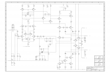
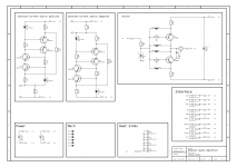
Here is also the schematic of the driver module.
This is basically like the folded driver in Bob Cordell's book (1st edition) figure 11.16.
The output stage is just a plain emitter follower with each four MJL3281 and MJL1302. 2R2 at the bases and 0.22R at the emitters. Nothing special really.
Maybe worth mentioning is that the output stage power supply is +/-22V and the bias is 3.7A roughly for class A operation. The front end and driver has its supplies elevated by 10V.
Attachments
Each of your current mirrors are a feedback network that could oscillate. Probe each one to see where signal is highest (or where the probe alters the oscillation the most).
(I can't see how the driver can work. You have collectors for npn, pnp connected together and they are being used as emitter followers. Say the input goes high, current flows into Q10 collector, it can't come from Q11. There collectors need to go to appropriate supply.)
(I can't see how the driver can work. You have collectors for npn, pnp connected together and they are being used as emitter followers. Say the input goes high, current flows into Q10 collector, it can't come from Q11. There collectors need to go to appropriate supply.)
Thanks for your comments.
2R2 as base stopper resistor is not uncommon for BJT output stages. The base resistor should not be higher than 10 times the emitter resistor. So this fits the 0R22 emitter resistors well.
You are right, for MOSFETs, several hundred Ohms at the gate are pretty common.
By popular request, please find attached schematic of the output stage.
As pointed out earlier, there is not so much special about the output stage. Maybe except the over-voltage protection that I have from Bob Cordell. Back when I designed this in, I had an idea why, but meanwhile I forgot the rationale behind. Probably, this could be simplified.
Attachments
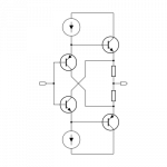
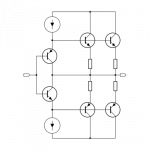
I will try to explain how the folded driver works:
This stems from my wish to build a powerful diamond output stage. So I started with the standard diamond buffer, which looks like this:

A better variant would be to connect the collectors of the driver transistors to the emitter resistors of the output transistors like this:

For driving multiple output transistors, this could be modified like this:

The driver transistors turn off the output transistors and the CCS are for turning them on.
When I got to this point, I found out that Bob Cordell has already described this in his book. He also added a small low pass filter from the output node back to the driver transistors common collector.
This small filter, R12 and C2 in my schematic, seems to be very important. Without this filter or with the filter not optimized, this is an excellent oscillator (the sine waves at 250kHz looked really good!).
Bob suggests 100R and 100pF in his book. In simulation I found that the resistor R12 affects DC offset and lowered it to 10R and increased C2 to 1nF. Should be the same in the end, but isn't.
Which brings us to the solution of the oscillation problem:
I increased R12 to 100R and this helped a lot.
I also experimented with increasing C2 to 10nF, but this slows down the output stage too much. I will go back to 1nF.
the DC offset is a problem in reality as well. My observation is that roughly each Ohm of R12 equals 1mV DC offset at the output. This means I have 100mV DC offset now, which is not good.
However, this is not a complete cure for the stability issue. The amplifier is stable now with the feedback loop closed after the front end. If I include the output stage in the feedback loop, there is still oscillation, but slightly damped instead of fully sustained and this is the case even with C2=10nF.
In general, I would not mind excluding the output stage from the feedback loop. Since this runs in class A, distortion is pretty low anyway. Whether this plays well together with any speakers connected, is another story then.
Getting the folded driver to work well seems challenging, but at least I have a forward path now and can go on summer vacation with a good feeling looking forward to continuing evaluation in a month.
This stems from my wish to build a powerful diamond output stage. So I started with the standard diamond buffer, which looks like this:
A better variant would be to connect the collectors of the driver transistors to the emitter resistors of the output transistors like this:
For driving multiple output transistors, this could be modified like this:
The driver transistors turn off the output transistors and the CCS are for turning them on.
When I got to this point, I found out that Bob Cordell has already described this in his book. He also added a small low pass filter from the output node back to the driver transistors common collector.
This small filter, R12 and C2 in my schematic, seems to be very important. Without this filter or with the filter not optimized, this is an excellent oscillator (the sine waves at 250kHz looked really good!).
Bob suggests 100R and 100pF in his book. In simulation I found that the resistor R12 affects DC offset and lowered it to 10R and increased C2 to 1nF. Should be the same in the end, but isn't.
Which brings us to the solution of the oscillation problem:
I increased R12 to 100R and this helped a lot.
I also experimented with increasing C2 to 10nF, but this slows down the output stage too much. I will go back to 1nF.
the DC offset is a problem in reality as well. My observation is that roughly each Ohm of R12 equals 1mV DC offset at the output. This means I have 100mV DC offset now, which is not good.
However, this is not a complete cure for the stability issue. The amplifier is stable now with the feedback loop closed after the front end. If I include the output stage in the feedback loop, there is still oscillation, but slightly damped instead of fully sustained and this is the case even with C2=10nF.
In general, I would not mind excluding the output stage from the feedback loop. Since this runs in class A, distortion is pretty low anyway. Whether this plays well together with any speakers connected, is another story then.
Getting the folded driver to work well seems challenging, but at least I have a forward path now and can go on summer vacation with a good feeling looking forward to continuing evaluation in a month.
Attachments
I haven't really understood the root cause of the problem, but found out that this R12 and C2 filter has a lot of impact. What strikes me is that reality disagrees with simulation here, which makes the phenomenon more difficult to examine.
The rationale behind why the folded driver may be something great is as follows:
The collector-emitter voltage across the driver transistors is very low and constant. This eliminates all kinds of Vce dependent non-linearity. Also, this presents a more constant load to the VAS (like constant Cbc).
In theory this arrangement also allows to use super fast small signal transistors, but in practice the driver transistors need thermal coupling with the output transistors to maintain stable DC bias in the output stage over varying temperature so packages with a mounting hole are beneficial. I measured DC bias and found that this works well in practice, too.
Note that this folded driver arrangement is suitable for class A output stages only in my opinion. It is difficult to get bias low enough for class AB operation and near impossible to maintain it at the optimal bias point. According to my measurement, it takes really long time for the bias to settle. This is due to the driver transistors being very far away from the output stage transistors and maybe could be improved by mounting them directly on top of the output stage transistors like one would mount a Vbe multiplier. This is just more challenging because I would not run long wires to the driver transistors, while this is acceptable for Vbe multipliers.
The drive to the output stage transistors is current limited, which may be a good thing, dependent on point of view.
Some flying catch diodes added around the driver transistors can serve as simple and effective overload management without affecting the performance too much.
Regarding the current sources:
Yes, they actually form some kind of feedback loop, but I believe this is without high gain and does not propose a significant risk for instability. One CCS feeds its output current through the other CCS reference element (i.e. LED here). The dependence of the CCS output current on the current through its reference element is there, but not so high.
Some other CCS like the ANF are pretty difficult to get stable, but the ones I use here seem pretty tame while (being cascoded) offering nearly the same performance like the ANF.
The mayor advantage of this type of CCS is hat the CCS current does not depend on the voltage across the CCS. The output impedance is high, especially with cascodes.
The cascodes in the current sources may go unstable. This is something I'm a bit afraid of and the reason why D1 to D4 in the driver module schematic are resistors. First I planned in diodes, but then changed my mind and installed resistors instead hoping that this damps any resonances that could occur in conjunction with circuit parasitic elements.
What I currently believe may be the root cause for the oscillation is that the front end output impedance and the driver/output stage input impedance conflict with each other somehow. So this may be a form of incompatibility of the stages with each other. Good I build this in a modular way so I can just swap the driver module for something else with little effort in case this one won't work well enough. It also seems that the common collector node condition of the driver stage somehow is "reflected" to the input node of the driver/output stage. All just weird speculation at this point. I have some weeks now to stay way from the problem long enough to speculate and make up all kinds of theories and probably understand it - or just enjoy my vacation.
This kind of issue is hard to solve.
A look in simulation files can help to find a solution, but as wrote it can fail.
As far I can understand the solution can be related with compensation. It can be a simple schema or you must need more than one point (or stage) to compensate. It is really a hard work that must be done in real amplifier.
Good Look and success.
Ronaldo
Hello nattawa,
that's a very good point indeed. Thanks for bringing this up.
The CCS source / sink 105mA.
And the output stage consumes quite a bit of idle current: Say each transistor has 1A bias and hfe is 50, then that's 20mA per transistor and 80mA total - just idle.
Chances are that this is insufficient.
that's a very good point indeed. Thanks for bringing this up.
The CCS source / sink 105mA.
And the output stage consumes quite a bit of idle current: Say each transistor has 1A bias and hfe is 50, then that's 20mA per transistor and 80mA total - just idle.
Chances are that this is insufficient.
- Home
- Amplifiers
- Solid State
- VFA front end - the Bunnyphant