The problem is the servo output filter. That’s an extra pole in the feedback path, which maps to a low frequency zero in the loop gain, hence the peaking.
If you insist in using this filter (not sure why you think it is needed here) you have to add a resistor in series with the servo op amp integrator capacitor. This will create a LF pole in the loop gain, and if this pole is at the same frequency with the filter zero they will compensate each other and the peak will vanish. Calculate the resistor by equating the two time constants above.
If you insist in using this filter (not sure why you think it is needed here) you have to add a resistor in series with the servo op amp integrator capacitor. This will create a LF pole in the loop gain, and if this pole is at the same frequency with the filter zero they will compensate each other and the peak will vanish. Calculate the resistor by equating the two time constants above.
Bob Cordell answer regarding the GAIA: https://www.diyaudio.com/forums/sol...lls-power-amplifier-book-527.html#post6768748
The problem is the servo output filter. That’s an extra pole in the feedback path, which maps to a low frequency zero in the loop gain, hence the peaking.
If you insist in using this filter (not sure why you think it is needed here) you have to add a resistor in series with the servo op amp integrator capacitor. This will create a LF pole in the loop gain, and if this pole is at the same frequency with the filter zero they will compensate each other and the peak will vanish. Calculate the resistor by equating the two time constants above.
Just included the servo in the NFB loop.... now there is no peaking in OLG.
I understand now my error.... Thank you again.
But I read some comments about filtering the output of the servo.... does it change the servo speed ?
Latest mods on the GAIA https://www.diyaudio.com/forums/sol...ral-mosfet-power-amplifier-3.html#post6763678
I am now used to the GAIA sound. It is important to get experienced with the amp sound with diverse sources before deciding the best tuning options.
This amp architecture is similar to the LIN but uses a differential TIS so it tends to clean 2nd harmonics.
Comparing the GAIA (Diff TIS) to the LIN (Blameless style amp) I noticed:
1- improvements in vocals intelligibility and reduced BOX effect on male voices
2- better articulation in female voices with reduced NASALTY
3- sweeter cymbals with very good extension and air
4- Less finger sound on bass and less guitar attack
5- Less low bass nitidity and deepness
To solve the identified issues (mainly in the bass and low mids on male voices) I experimented with the compensation and also the input stage cascode emitter resistors.
I was using the following TMC values: 100p - 470p - 1k8ohm (resulting in 82.5p for miller)
Now using 100p - 500p - 1k8ohm (83.3p miller comp)
R5 and R8 are used to minimize power fluctuations in the input jfets while slightly reducing HF distortion but they tend to smooth the sound picture.
Without these resistors I completely solved issues 4 and 5
Now bass goes deep with high definition and there are improvements in guitar attack and finger pluck in stringed instruments.
Now presenting the RCP130 KALI EVO47.728
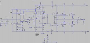
A folded cascode IPS based on the AD826 chip.
This architecture provides wide bandwidth with very high slew rate.
Low noise is assured by the choice of low input and feedback resistances.
A folded cascode IPS based on the AD826 chip.
This architecture provides wide bandwidth with very high slew rate.
Low noise is assured by the choice of low input and feedback resistances.
Attachments
KALI Schematic
KALI SCH....
Note noise reduction choices:
Input R28 = 470 ohm
NFB R19 = 9k8 ohm
Driven cascode:
The bases of the IPS cascode are referenced to the input signal using a pnp (Q16) with the base connected to the jfets sources.
Cascoded IPS CCS:
Q3 (NPN current setting bjt) is cascoded by Q14 greatly increasing the CCS output impedance and PSRR.
Non intrusive offset control:
D10 / D16 and the surrounding resistors provide a temperature compensated offset control (based on KRELL design).
Balanced VAS operation:
Q4 PNP cascode is used to minimise voltage differences between the collectors of the folded cascode Q5 Q6, keeping their power dissipation in similar levels.
Attachments
Thank you Hugh
It does sound good this one")
Q3 npn is the CCS control bjt. (BC550C chosen due to it's ability to work well with very low Vce)
The CCS is done by fixing the base voltage using a LED as reference. This voltage is than filtered with R5 (100ohm) and C12 (220u) to minimize noise but principally to keep the base of Q3 steady. (This arrangement also produces higher CCS output impedance.
The CCS is then cascoded by a medium power npn (Q3) where it's base is fixed by the voltage set by D5 + D6.
R17 is a base stopper for Q14
R6 on top of the CCS minimizes capacitive interactions between the CCS and IPS sources and removes power on thump.
Current for the voltage references D5 D6 is set by R10 (33k) that is referenced to the V++ rail so to not pollute GND in any way.
It does sound good this one
Q3 npn is the CCS control bjt. (BC550C chosen due to it's ability to work well with very low Vce)
The CCS is done by fixing the base voltage using a LED as reference. This voltage is than filtered with R5 (100ohm) and C12 (220u) to minimize noise but principally to keep the base of Q3 steady. (This arrangement also produces higher CCS output impedance.
The CCS is then cascoded by a medium power npn (Q3) where it's base is fixed by the voltage set by D5 + D6.
R17 is a base stopper for Q14
R6 on top of the CCS minimizes capacitive interactions between the CCS and IPS sources and removes power on thump.
Current for the voltage references D5 D6 is set by R10 (33k) that is referenced to the V++ rail so to not pollute GND in any way.
- Home
- Amplifiers
- Solid State
- RCP130 modular lateral mosfet power amplifier