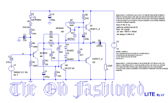
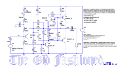
Some time ago, Daniel asked me if I could design "discrete chipamps", ie. amplifiers as simple, tolerant and easy as chipamps, but completely discrete in the seventies style, and with additional constraints: single-supply, no LTP, no unusual parts like lat-FETs and transistor count < 9.
Here is the result for the lite version: ~0 to 25W output.
It is the base circuit: the circuit lends itself to various modifications and improvements (will be described later).

It is built to be highly flexible and tolerant: it was initially designed for supply voltages ranging from 3.3V to 24V without any component change, but it can in fact work from less than 3V to more than 30V if the capacitors have a sufficient voltage rating.
All components are non-critical, and it can work with cheap internet parts (my prototype uses some).
The performances are not exceptional, but they are decent enough for such a small circuit, and normally sufficient for most applications.
Since the thermal compensation/quiescent current is always a delicate issue for DIY amps, it uses an automatic class-B bias engine: no adjustment, and only basic thermal coupling is required (this can even be dispensed with completely, more on that later).
The efficiency is also quite good: with a 19V supply, it manages to deliver 18Vpp into a 4Ω load.
The schematic and sim use the D44/D45 OP pair, because it was a preference of Daniel, but in my build I used a BD435 from ST and a BD438 from Philips. Not the best match, but it works with this amp. The VAS is not a BC337, but a CN made S8050.
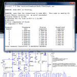
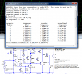
The simmed THD is 0.04%, against 0.05% in reality.
The power bandwidth exceeds 300kHz.
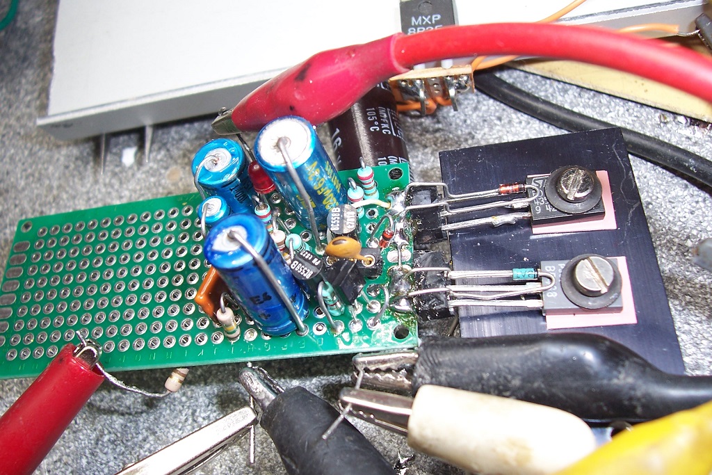
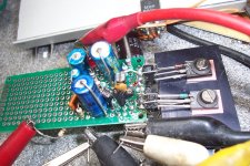
Here is a pic of the prototype:
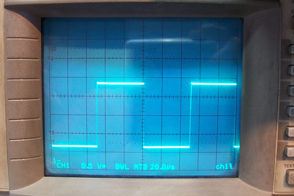
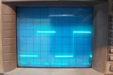
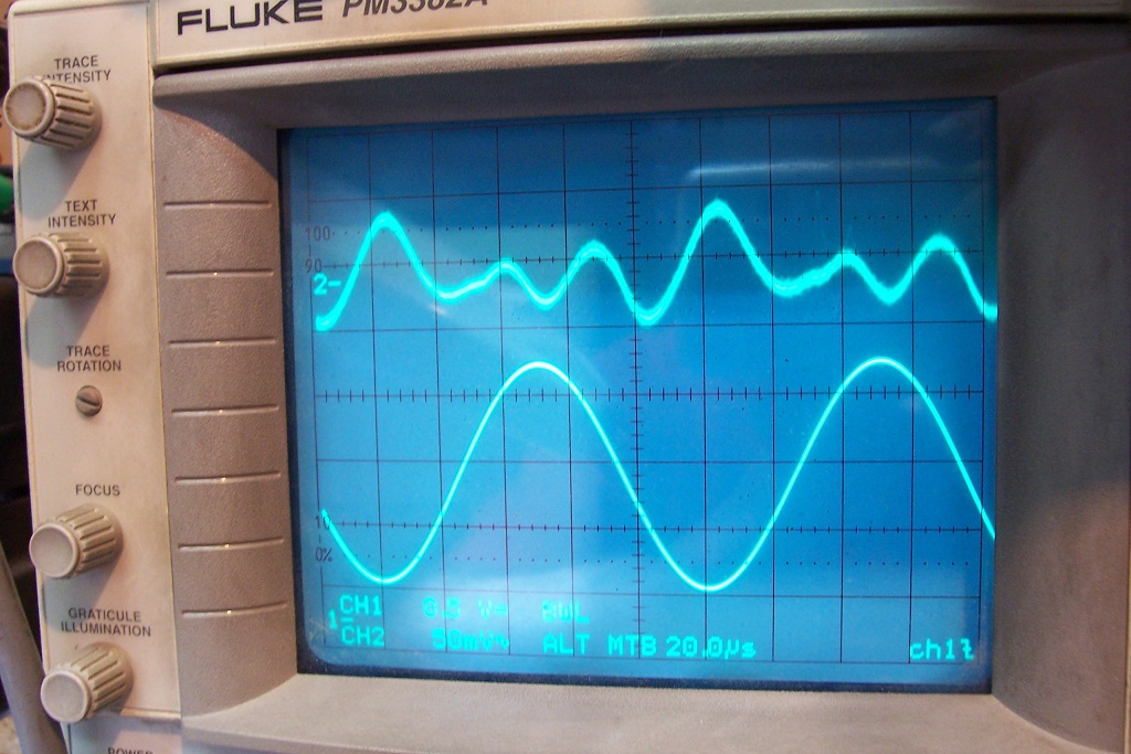
And here is the 10kHz, large-signal squarewave response:
Here is the result for the lite version: ~0 to 25W output.
It is the base circuit: the circuit lends itself to various modifications and improvements (will be described later).
It is built to be highly flexible and tolerant: it was initially designed for supply voltages ranging from 3.3V to 24V without any component change, but it can in fact work from less than 3V to more than 30V if the capacitors have a sufficient voltage rating.
All components are non-critical, and it can work with cheap internet parts (my prototype uses some).
The performances are not exceptional, but they are decent enough for such a small circuit, and normally sufficient for most applications.
Since the thermal compensation/quiescent current is always a delicate issue for DIY amps, it uses an automatic class-B bias engine: no adjustment, and only basic thermal coupling is required (this can even be dispensed with completely, more on that later).
The efficiency is also quite good: with a 19V supply, it manages to deliver 18Vpp into a 4Ω load.
The schematic and sim use the D44/D45 OP pair, because it was a preference of Daniel, but in my build I used a BD435 from ST and a BD438 from Philips. Not the best match, but it works with this amp. The VAS is not a BC337, but a CN made S8050.
The simmed THD is 0.04%, against 0.05% in reality.
The power bandwidth exceeds 300kHz.
Here is a pic of the prototype:
And here is the 10kHz, large-signal squarewave response:
Attachments
Last edited:
Amazing performance 12.6 Vav from 19 v in. 19vdc is about the cheapest available 50 w supply these days from the laptop computer vendors. .05% HD is great, 100 times better than HD of most cheap speakers.
Only exotic part is the BAT54?? What voltage & wattage zener? I've got some original 197? GE D44R2 transistors from the NY production line.
Great step forwards for the newby protecting amp with speaker cap class. Mess up something, the amp sits there and nothing happens but heat. No new speaker required.
Last edited:
Only exotic part is the BAT54?? What voltage & wattage zener?
Have another look at the schematic symbol. Check the datasheet. BAT54 is not a zener.
I have taught myself how to solder SOT23-3 packaged semiconductors, it didn't take very long and I didn't make very many fatal soldering errors.
In my opinion, SOT23-3 components are going to keep growing, as a percentage of total components shipped. And thru hole components are going to keep decreasing, as a percentage of total components shipped. Of course these are nothing more than my own personal GUESSES; the future may not play out in exactly the way that I have forecasted!
Best wishes to all,
no unusual parts like lat-FETs and transistor count < 9.
A led is an unusual part in an audio amplifier. A FET is a usual part in an audio amplifier.
It is a great classic of the seventiesNice work!!
The bootstrap C4 is a good idea.
Here it is for 1WCan you please show predicted distortion profile for 1kHz st say 1w and 8w into 8ohms?
And for 8W
Not exactly exotic: as I was a bit lazy, I took the first small-current schottky available in LTspice.Only exotic part is the BAT54?? What voltage & wattage zener? I've got some original 197? GE D44R2 transistors from the NY production line.
In fact any small (100~300mA) schottky's like BAT42, BAT48, BAT85 etc will also work, and those are leaded.
There are also 1Nxxxx and 1Sxxx alternatives.
Do not use higher current devices like 1N5818.
Now, here are important informations for those wanting to experiment with the circuit: its mode of operation is rather disconcerting.
It is not a class AB amplifier: it manages to be a switching and non-switching class B amp at the same time.
This explains the absence of emitter resistors (and the resulting efficiency)
The quiescent current is not adjustable: it is set internally by the components parameters, namely the β ratio of Q3 and Q1 and the current through R7 and R8.
For example, if β(Q1)/β(Q3)=1, the quiescent current of the output will mirror that of R7, R8: Iq= (Vs/2)/(R7+R8).
The diodes D1 to D3 have no influence on the quiescent current, yet D1 and D2 have to (grossly) track the temperature of Q1 and Q2.
Since the β of Q3 has an influence on the quiescent current, it is preferable to make it also track that temperature.
From the pic, you can see that I didn't follow very seriously my own advices: the diodes are just in the vicinity of the transistors leads, and Q3 is simply left on the board.
This why the current build uses a 1N4148 + BAT43.
It worked with the 1N4002's, but when I made tests at higher voltages, it triggered a thermal runaway.
In theory, it slightly degrades the performances, but the effect is minimal and the measurements and screenshots were taken in those conditions
To get acquainted with the circuit, for example by building it on a breadboard with improvised external heatsinks and diodes remaining very far on the breadboard, you need to take one of these safety measures:
-Short D1 or D2 or even both
-If the diodes are not too far from the transistors, you can shunt (or replace) one of them by a schottky (that's what you can see in the pic of my prototype).
Without these measures and a haphazard thermal construction, the result will be a quick and irrecoverable thermal runaway.
Note that for the tests, the circuit can run completely normally (and safely) without D1, D2 and D3: it will simply result in detectable crossover artifacts, but other than that it will operate normally, and completely safely
Attachments
Last edited:
Good work! Thanks to projects like this I became interested enough to investigate the ROI (Return Of Investment) regarding LTP, symmetrical versions of them, drivers, driving methods, error correction etc. In the course of events it became clear that the "classic 1970 style" amp as it's called here, fitted with the proper components, could even be made to perform at the 200W (4 ohm) level with just under 1 ppm (mostly 2nd harmonic) distortion.
No, as I said above, it cannot be a large, rectifier type. It has to be a signal one.I would hope an MBR1100 schottky diode would work. This is a leaded component stocked at farnell US with 0.4 Vf @ 20 ma and 1.0 @ 1 A.
But you can provisionally omit it completely for the moment, and install it later when you have found something suitable.
Well, let's say mildly unusual. If it is a problem, just stack 3 1N4148.A led is an unusual part in an audio amplifier. A FET is a usual part in an audio amplifier.
And Daniel preferred it with no FETs.
") , not in the main PCB.
, not in the main PCB.SIC: "It’s quite common actually"
But not too common in classic/vintage circuits. I had repaired lots of old fashioned amps like the classic AD161-162 pair, the quasi made from AD149, and so on, and no led's at all, the main power indicator usually was a 6.3V #40 or #47 lamp.
But not too common in classic/vintage circuits. I had repaired lots of old fashioned amps like the classic AD161-162 pair, the quasi made from AD149, and so on, and no led's at all, the main power indicator usually was a 6.3V #40 or #47 lamp.
The "twist" is mainly elsewhere: it is in the class B steering system.
That said, the topology could easily adapt itself to purely Ge devices: it works from first principles, and that remains true whatever the bandgap of active devices is.
One could also make a hybrid Ge/Si build.
Here is a description of how the circuit works, but first, this is the schematic drawn like it should have been, with the desirable thermal couplings shown explicitly.
Note that D3 is excluded, and that's how it should be.
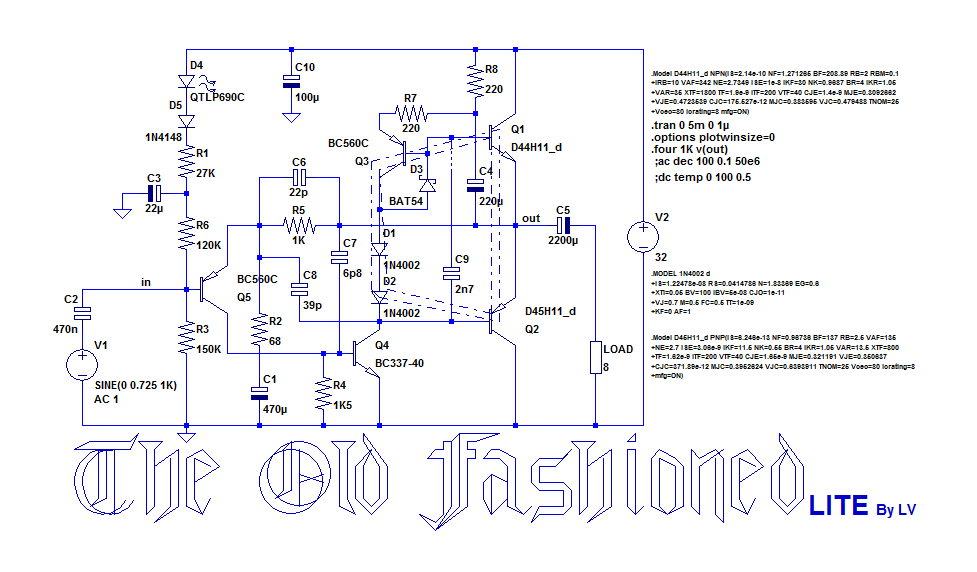
Under quiescent conditions, the main loop imposes a DC voltage of Vs/2 to the "out" node.
The emitter of Q3 will thus sit at 2Vbe above that, creating a current through R7, R8 and the emitter.
This emitter current will require a base current, imposed by Q3's β.
This will create an emitter current in Q1, but because of the main loop, Q4 will draw a current just sufficient to balance Q3's collector current, plus the base current of Q2 required to maintain the stasis.
A steady quiescent current is thus created, provided Q3 has enough C-E room to maintain it.
Without D1 and D2, this condition is obviously met.
With D1 and D2 adding two Vbe into the equation, the condition is still met, because Q3 can pull the anode of D1 practically one Vbe more positive than the base of Q1.
With the antisaturation diode D3 thrown into the problem, the condition can still be met, because being a schottky, it will spend only ~half an additional Vbe.
If a positive output excursion is required, Q4's collector current will not match the current imposed by R7, R8, causing Q3 Vce to collapse until the antisaturation diode D3 kicks into action, shunting the excess current towards the base of Q1, driving it into conduction.
If a negative excursion is required, Q4's collector current will exceed what R7, R8 can provide, and this excess current will drive Q2 into conduction.
To sum up: Q1 will always conduct, even during its "quiescent" time, but the conduction of Q2 will be hard-switched, depending on the need: this is why the circuit is both switching and non-switching.
The switching aspect might seem to be a potential source of artifacts and discontinuities, but this is mitigated by the fact that Q1 remains always in conduction, thus keeping a certain control on the output, and the role of D1 to D3 is to reduce the magnitude of the discontinuity from ~3Vbe to 100 or 200mV.
It would be easy to keep both Q1 and Q2 in conduction all the time: simply add the N counterpart of Q3 to the base of Q2.
In reality, there is not much benefit in doing that: firstly, it consumes one Vbe on the non-bootstrapped side, reducing the output swing and the low-voltage operation ability, and secondly, it is not necessary: with a step of 100 to 200 or 300mV, the output is able to "ride over" the trough thanks to stored charge and similar effects, and the fact that the phenomenon is completely local, just confined between the collectors of Q3 and Q4, not relying on GNFB, thus very fast.
This is confirmed by the THD residue, where no Xover artifact is visible.
When one of the diode is shorted, small artifacts become visible on the waveform, but the global THD figure remains utterly unchanged.
Thus, it is important to minimize the step, and the magnitude of the step depends on the OP's temperature, which is why minimal thermal tracking is necessary.
Without thermal tracking, things can quickly turn sour because there are no emitter resistors.
Without the various control diodes, the circuit still works, and it does not even require thermal tracking, but the transistor's saturation sticking and the magnitude of the step generate some Xover artifacts, perfectly tolerable for PA or communication channels, but not acceptable for HiFi
That said, the topology could easily adapt itself to purely Ge devices: it works from first principles, and that remains true whatever the bandgap of active devices is.
One could also make a hybrid Ge/Si build.
Here is a description of how the circuit works, but first, this is the schematic drawn like it should have been, with the desirable thermal couplings shown explicitly.
Note that D3 is excluded, and that's how it should be.
Under quiescent conditions, the main loop imposes a DC voltage of Vs/2 to the "out" node.
The emitter of Q3 will thus sit at 2Vbe above that, creating a current through R7, R8 and the emitter.
This emitter current will require a base current, imposed by Q3's β.
This will create an emitter current in Q1, but because of the main loop, Q4 will draw a current just sufficient to balance Q3's collector current, plus the base current of Q2 required to maintain the stasis.
A steady quiescent current is thus created, provided Q3 has enough C-E room to maintain it.
Without D1 and D2, this condition is obviously met.
With D1 and D2 adding two Vbe into the equation, the condition is still met, because Q3 can pull the anode of D1 practically one Vbe more positive than the base of Q1.
With the antisaturation diode D3 thrown into the problem, the condition can still be met, because being a schottky, it will spend only ~half an additional Vbe.
If a positive output excursion is required, Q4's collector current will not match the current imposed by R7, R8, causing Q3 Vce to collapse until the antisaturation diode D3 kicks into action, shunting the excess current towards the base of Q1, driving it into conduction.
If a negative excursion is required, Q4's collector current will exceed what R7, R8 can provide, and this excess current will drive Q2 into conduction.
To sum up: Q1 will always conduct, even during its "quiescent" time, but the conduction of Q2 will be hard-switched, depending on the need: this is why the circuit is both switching and non-switching.
The switching aspect might seem to be a potential source of artifacts and discontinuities, but this is mitigated by the fact that Q1 remains always in conduction, thus keeping a certain control on the output, and the role of D1 to D3 is to reduce the magnitude of the discontinuity from ~3Vbe to 100 or 200mV.
It would be easy to keep both Q1 and Q2 in conduction all the time: simply add the N counterpart of Q3 to the base of Q2.
In reality, there is not much benefit in doing that: firstly, it consumes one Vbe on the non-bootstrapped side, reducing the output swing and the low-voltage operation ability, and secondly, it is not necessary: with a step of 100 to 200 or 300mV, the output is able to "ride over" the trough thanks to stored charge and similar effects, and the fact that the phenomenon is completely local, just confined between the collectors of Q3 and Q4, not relying on GNFB, thus very fast.
This is confirmed by the THD residue, where no Xover artifact is visible.
When one of the diode is shorted, small artifacts become visible on the waveform, but the global THD figure remains utterly unchanged.
Thus, it is important to minimize the step, and the magnitude of the step depends on the OP's temperature, which is why minimal thermal tracking is necessary.
Without thermal tracking, things can quickly turn sour because there are no emitter resistors.
Without the various control diodes, the circuit still works, and it does not even require thermal tracking, but the transistor's saturation sticking and the magnitude of the step generate some Xover artifacts, perfectly tolerable for PA or communication channels, but not acceptable for HiFi
Attachments
Last edited:
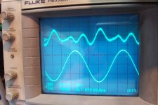
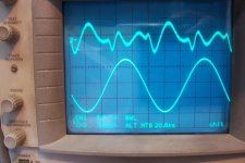
To illustrate what I said earlier about the diodes, here are the THD residues (0.05%) waveforms with the circuit in normal working order, ie. D1 & D2 in circuit, and with one of the diodes shorted.
With D1 & D2:
With D1 shorted:

The first is clearly preferable for normal operation, but for completely safe tests, tweaking and debugging, the quality of the second is ample enough.
The optional capacitor C9 slightly improves the situation for the degraded mode, because it provides a feedforward path from one base to the other, helping the transistors keep the control over the output signal.
For normal operation, its effect is nil.
With D1 & D2:
With D1 shorted:
The first is clearly preferable for normal operation, but for completely safe tests, tweaking and debugging, the quality of the second is ample enough.
The optional capacitor C9 slightly improves the situation for the degraded mode, because it provides a feedforward path from one base to the other, helping the transistors keep the control over the output signal.
For normal operation, its effect is nil.
Attachments
- Home
- Amplifiers
- Solid State
- Old-fashioned amplifiers with a new twist (1)