Hi stocktrader200,
Trust me, if I had the cash, I would be working on a rebuild right now, or enjoying the amplifier.
Luckily I do have access to some amplifiers I have rebuilt for some people and could literally copy the PCBs. That would require an extreme amount of trust in me. Some have even suggested this line of action.
Most importantly, the amount of custom metal work required will be crushingly expensive, not to mention the extreme commitment in time. Never mind the custom faceplate and meters. I know where I can obtain custom meters, so that isn't a problem.
The end result would be one hideously expensive amplifier. I have even checked with Hammond Manufacturing and have a (very) rough quote for the 2.2 KW transformer. Hammond is *very* DIY friendly.
No, the least expensive route to get what I want is to buy a Marantz 500, then strip and rebuild it. I've wanted one since the time I first serviced one my way in the 1980's. After I did the first upgraded rebuild I really wanted one. After the last update improved the sound quality even more, the desire to own one is much stronger. What can I say?
One of the earliest upgrades I made was to match the output transistors more tightly than the factory specified. Somewhere in the service manual the actual range of Beta values has been given for anyone who would like to argue that point some more. You just will not argue with me on it. Remember, the factory specifications are so that the amplifier performs at some minimal level to satisfy the published specifications. We can always do better. If I'm already removing the outputs in order to check and grade them, why not do better and match them?
The first amps I created matches from the pool of two sets of outputs (both channels) and ordering new ones to replace the flyers. That improved performance. Soon after I was ordering sets of new transistors and matching them more tightly, and comments back from customers proved we were on the right track. Never mind the lower distortion readings. I'm just passing on the experience of all those years of doing this kind of work.
I miss the years when the general consensus was that Marantz was junk. Prices were reasonable. Then it was discovered that certain industry mouthpieces were absolutely wrong about Marantz. Now I can't afford the brand that I like so much as I think prices have overshot the actual worth. Especially for what passes as a "restoration" by people who aren't technicians. Just greed.
-Chris
Trust me, if I had the cash, I would be working on a rebuild right now, or enjoying the amplifier.
Well, mostly because performance is directly related to the PCB layout for one. That and not all of the original parts are available in the original case styles. If I were to attempt to create a modern version, I would use current components.Why not make up some boards off the schematics and place it all in a DIY case. It won't be an original but it won't cost you 6- 7 grand either.
Luckily I do have access to some amplifiers I have rebuilt for some people and could literally copy the PCBs. That would require an extreme amount of trust in me. Some have even suggested this line of action.
Most importantly, the amount of custom metal work required will be crushingly expensive, not to mention the extreme commitment in time. Never mind the custom faceplate and meters. I know where I can obtain custom meters, so that isn't a problem.
The end result would be one hideously expensive amplifier. I have even checked with Hammond Manufacturing and have a (very) rough quote for the 2.2 KW transformer. Hammond is *very* DIY friendly.
No, the least expensive route to get what I want is to buy a Marantz 500, then strip and rebuild it. I've wanted one since the time I first serviced one my way in the 1980's. After I did the first upgraded rebuild I really wanted one. After the last update improved the sound quality even more, the desire to own one is much stronger. What can I say?
One of the earliest upgrades I made was to match the output transistors more tightly than the factory specified. Somewhere in the service manual the actual range of Beta values has been given for anyone who would like to argue that point some more. You just will not argue with me on it. Remember, the factory specifications are so that the amplifier performs at some minimal level to satisfy the published specifications. We can always do better. If I'm already removing the outputs in order to check and grade them, why not do better and match them?
The first amps I created matches from the pool of two sets of outputs (both channels) and ordering new ones to replace the flyers. That improved performance. Soon after I was ordering sets of new transistors and matching them more tightly, and comments back from customers proved we were on the right track. Never mind the lower distortion readings. I'm just passing on the experience of all those years of doing this kind of work.
I miss the years when the general consensus was that Marantz was junk. Prices were reasonable. Then it was discovered that certain industry mouthpieces were absolutely wrong about Marantz. Now I can't afford the brand that I like so much as I think prices have overshot the actual worth. Especially for what passes as a "restoration" by people who aren't technicians. Just greed.
-Chris
Hi mjona,
Yes, absolutely. However, that just means that obtaining matched sets can be done at a lower cost. If you can, matching is a "tweak" that you can do easily for yourself.
-Chris
I have not built an amplifier having parallel pairs of output transistors so for me any matching exercise would be of complementary pairs.
You reported a 20 dB claimed improvement with MJL21195/MJL21196 at 1kHz, 100W into 8R at 1kHz.
The data sheet for MJL21193/MJL21194 makes the same claim and Bob Cordell has .models for these on his website and a simulation using such was an interesting thought. I made the THD to be of the order of 0.08% at 100W into 8R.
The accuracy may enable dc behaviour at Ic levels other than 5A to be predicted and in reality targetted by some simple test means.
That suggests a vast improvement in semiconductor design and manufacture between 1973 and 2017.
I worked in the semiconductor manufacturing field in the equipment engineering groups for about 22 years. First for SGS-Thomson from 1988-1992 and then for National Semi from 1992 - 2010, when we closed down the Nat'l Semi Arlington manufacturing fab. I supported ion implanters at first and later in my career I moved to thin films deposition systems i.e. metallization (sputtering) & PE-CVD, mostly high vacuum equipment. I can attest that in that period of time the manufacturing side of the field has changed dramatically. Process control was present in the 80's but became much more intensified and broad as time wore on. The manufacturing equipment also matured greatly in that time. Process uniformity across the ever larger wafers has steadily improved. Now its common for center to edge wafer process uniformity to be better than 1%, three decades back the acceptable uniformity across the wafer could be many times that number.
My father worked in the same field for TI on the process side from 1973 - 1995 and his take on the manufacturing changes he experienced is even more extreme.
Hi mjona,
Matching the like transistors for each polarity also reduces distortion in that it allows them to operate as one and remain under control of the circuit. Having a random and soft transition from not conducting to conducting isn't going to help having a smooth changeover from the PNP half to the NPN half.
Hi Chamberman,
With normal output transistors I see these days, the beta counts are much more random and matching is still beneficial. I would love a day where I didn't have to match parts! The signal transistors have also improved a great deal, but the variance is still too great to just pluck them out of a bag or drawer and use them in pairs. Better than in the 70's for sure, but we aren't there yet. Beta variations are much greater with signal transistors than the power types. I wonder if that is simply due to the fact that we are dealing with higher transconductance devices, or just the smaller die size? You would have the experience to shed some light on that issue.
- Chris
That was their test parameters. The reduction in THD holds for lower powers and is before adding feedback - so valid for a Stassis type amplifier of any other design that excludes the output section from the feedback loop. When you add feedback, there is still a great reduction in distortion since the diff pair has less correction to do. The amount of reduction depends upon how far the outputs were from being matched to begin with. The important thing I'm trying to get across to people is that matching matters and isn't an expensive way to reduce distortion in their builds. Transistors that didn't match can be used in other projects - so minimal loss there.You reported a 20 dB claimed improvement with MJL21195/MJL21196 at 1kHz, 100W into 8R at 1kHz.
Matching the like transistors for each polarity also reduces distortion in that it allows them to operate as one and remain under control of the circuit. Having a random and soft transition from not conducting to conducting isn't going to help having a smooth changeover from the PNP half to the NPN half.
Hi Chamberman,
While I can't dispute your numbers, and will not attempt to do that, I think that uniformity across the wafer may not hold true for the larger geometry in discrete parts like transistors. Especially power transistors. The one time I did see uniformity like that (On Semi MJW0281 / MJW0302), the devices were discontinued. That was a very sad event for me. Common were beta figures in the 100 range varying only a few counts. Flyers were maybe 4 counts off average. Those parts were a dream come true for me. I was prepared to pay more for those parts had they remained in production.Now its common for center to edge wafer process uniformity to be better than 1%, three decades back the acceptable uniformity across the wafer could be many times that number.
With normal output transistors I see these days, the beta counts are much more random and matching is still beneficial. I would love a day where I didn't have to match parts! The signal transistors have also improved a great deal, but the variance is still too great to just pluck them out of a bag or drawer and use them in pairs. Better than in the 70's for sure, but we aren't there yet. Beta variations are much greater with signal transistors than the power types. I wonder if that is simply due to the fact that we are dealing with higher transconductance devices, or just the smaller die size? You would have the experience to shed some light on that issue.
- Chris
A convoluted argument to persist in the THD reduction from output transistor matching.The reduction in THD holds for lower powers and is before adding feedback - so valid for a Stassis type amplifier of any other design that excludes the output section from the feedback loop. When you add feedback, there is still a great reduction in distortion since the diff pair has less correction to do. The amount of reduction depends upon how far the outputs were from being matched to begin with.
- Chris
Most amplifier do use feedback. The no feedback stuff is another questionable fad.
Indeed when you add feedback there is a great reduction in distortion, however the output transistor mismatch is swamped by other non linearities.
Matching complementaries, at best removes even harmonics.
Tough luck, the odd harmonics are still there, feedback only, can reduce them.
Matching for load sharing, will not remove transistor non linearities, feedback only, can reduce them
Rod Elliot is right about this THD bit. His site is not as you've said. His site is great and he is good at debunking audio myths.Elliott Sound Products - The Audio Pages (Main Index)
Some Simulation Stuff
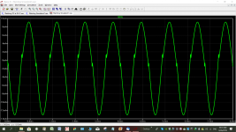
I did have two takes on the test set up in my simulation.
The datasheet circuit - with series blocks including a source amplifier and the AP1 test equipment in the chain. I could not include these unknowns but gave this a shot without them.
I found when looking at the current across the 50R series feed resistor there were notches in the sine wave which were not apparent at 40 peak voltage outputs. However if the input voltage to the power transistors was reduced these notches then appeared in the output wave form and the THD % increased.
Having been 0.524% at 100W a reduction to 1W resulted in an increase to 3.38%.
No doubt the source amplifier includes a feedback loop, and this would make those results look better if it was possible to include this circuit block.
Ignoring such benefits, working at low power levels uncovers a dead band in the cross-over region and my second attempt I saw fit to bias the power devices to cover the gap. V4 can be adjusted to test other bias levels.
The modified circuit is still notional but it did obviate the notches and reduce the THD by 20 dB at 100W. At a level of 1W this did creep back up a little but feedback should handle this in a fully worked power amp circuit.
Feel free to experiment with or make changes to either simulation.
Attachments
Hi mjona.
First circuit, bias is no good.
Your second circuit is on the way to a decent power amplifier.
Add an Op amp LTC6090 in front to drive the bases of your output transistors, then with a couple of resistors apply feedback. Then your are on the way to low THD.
First circuit, bias is no good.
Your second circuit is on the way to a decent power amplifier.
Add an Op amp LTC6090 in front to drive the bases of your output transistors, then with a couple of resistors apply feedback. Then your are on the way to low THD.
Last edited:
Seriously Chris, you are disputing a retired semi process engineer.I think that uniformity across the wafer may not hold true for the larger geometry in discrete parts like transistors. Especially power transistors.
The process improvements are shown in that they have discontinued most of the hfe grading of parts since they are all relatively the same with little variation.
Hi rsavas,
Actually, I'm not disputing him at all. I'm pointing out that it appears that the uniformity across the wafer for discrete transistors may not be that uniform. I suspect the controls are much tighter across wafers destined for high cost semis where the costs of non-uniformity is lower for discretes, that's all. Otherwise my own empirical observations agree with and are explained by what mchambin said. At the most, I merely questioned the degree of uniformity for products that were likely not his speciality. I agree wholeheartedly with him where integrated circuits are concerned. I do recognise that his knowledge and experience greatly outstrips any that I could even boast about (which I am not).
I constantly test and grade transistors as a normal course of what I do. I also re-run my experiments concerning distortion and transistor matching. What mjona pointed out was quite correct in that measured distortion does increase as the power is reduced in almost any well designed solid state power amplifier. Adding feedback does not negate the need for matching. It only reduces the range of distortion as absolute numbers. What I have measured suggests that the percent reduction of distortion remains more or less constant whether feedback is used, or not. So that means that you might be comparing 0.001% for matched vs 0.0025% for unmatched. Maybe greater, but I'm just giving reasonable numbers.
One thing I have seen is a reduction in the normal distortion we look for accompanied all kinds of what looks to be spurious signals. So what I'm trying to say is that the noise floor looks a lot cleaner in amplifiers with matched parts. Not all, but enough of them so that I'm watching to see if anything will correlate with those observations.
Finally, the first sentence of that post you are referring to began with this:
Best, Chris
Actually, I'm not disputing him at all. I'm pointing out that it appears that the uniformity across the wafer for discrete transistors may not be that uniform. I suspect the controls are much tighter across wafers destined for high cost semis where the costs of non-uniformity is lower for discretes, that's all. Otherwise my own empirical observations agree with and are explained by what mchambin said. At the most, I merely questioned the degree of uniformity for products that were likely not his speciality. I agree wholeheartedly with him where integrated circuits are concerned. I do recognise that his knowledge and experience greatly outstrips any that I could even boast about (which I am not).
Well, I wouldn't go that far actually. Just like in the 70's where most manufacturers did not grade their parts due to cost. it was a financial decision more than anything - and the acceptance of lower product performance. A few notable companies did grade their parts as it was required to obtain the performance they were claiming. Today it is very much the same question, costs vs performance. The difference, as you pointed out, is that the costs of not grading the parts are not nearly as dear as they used to be.The process improvements are shown in that they have discontinued most of the hfe grading of parts since they are all relatively the same with little variation.
I constantly test and grade transistors as a normal course of what I do. I also re-run my experiments concerning distortion and transistor matching. What mjona pointed out was quite correct in that measured distortion does increase as the power is reduced in almost any well designed solid state power amplifier. Adding feedback does not negate the need for matching. It only reduces the range of distortion as absolute numbers. What I have measured suggests that the percent reduction of distortion remains more or less constant whether feedback is used, or not. So that means that you might be comparing 0.001% for matched vs 0.0025% for unmatched. Maybe greater, but I'm just giving reasonable numbers.
One thing I have seen is a reduction in the normal distortion we look for accompanied all kinds of what looks to be spurious signals. So what I'm trying to say is that the noise floor looks a lot cleaner in amplifiers with matched parts. Not all, but enough of them so that I'm watching to see if anything will correlate with those observations.
Finally, the first sentence of that post you are referring to began with this:
I am not disputing what mchambin had to say, but my observations differed a little bit and I was just raising that point. Nicely I thought, not as an argument, but maybe it was taken that way.While I can't dispute your numbers, and will not attempt to do that, I think that uniformity across the wafer may not hold true for the larger geometry in discrete parts like transistors.
Best, Chris
Chris,
I see you making assumptions about stuff i am not sure if you are qualified to make about semiconductor processing.
I do not know how you can differentiate between uniformity of an IC vs a bjt on a wafer?
You can build your amps as you see fit if you think matching o/p devices matters to the degree in which you state.
I am looking at the marantz 500, interesting design, not sure it would be one that i would call my holy grail, input ef with CC load, asymmetric input diff pair which adds even order THD, and I just got started, it does look nice and has a beefy supply, a nice relic. I liked the Yamaha P-2200 that I was repairing.
I see you making assumptions about stuff i am not sure if you are qualified to make about semiconductor processing.
You are making another assumption about the persons specialty and experiences.At the most, I merely questioned the degree of uniformity for products that were likely not his speciality. I agree wholeheartedly with him where integrated circuits are concerned.
I do not know how you can differentiate between uniformity of an IC vs a bjt on a wafer?
You can build your amps as you see fit if you think matching o/p devices matters to the degree in which you state.
I am looking at the marantz 500, interesting design, not sure it would be one that i would call my holy grail, input ef with CC load, asymmetric input diff pair which adds even order THD, and I just got started, it does look nice and has a beefy supply, a nice relic. I liked the Yamaha P-2200 that I was repairing.
Last edited:
Hi mchambin,
I have purposely built amplifiers with matched outputs on one channel and unmatched ones on the other. The unmatched sets were pulled from sets of transistors purchased at the same time and graded. Therefore I knew what parts were being used where. In every case the unmatched sets always had higher distortion and some folks were able to hear these things. I never comment on my own work, leaving that to friends that are kept in the dark as to what has been done. Sometimes there is no matching in either channel, and sometimes in both. They never know what I've done. I'm just doing my best to match up opinion to measurements.
All I'm doing is looking at written application notes and applying what I read. My observations have always been made with the use of test equipment. It's always the best I can afford and would dearly love to own an AP or Keysight U8903B. I do own and use daily a wonderful device called an RTX 6001. It has really helped me make better observations. So anything I have said thus far is directly related to what I have been measuring. Maybe my conclusions are a little off, but not the observations. Nothing I have said is a thought experiment either, unlike some folks around here. If you can explain my observations I would be more than happy to consider them. I'm not afraid of being wrong (but would much rather be correct!). The observations I have made cannot be debunked as they are just that, observations made on physical amplifiers with the changes I made as I have reported. It's all just dry factual stuff from where I sit.
-Chris
I obviously disagree with you on that point. I have to go by what I'm actually seeing and measuring. To ignore this would be pretty darned silly and if you were in my shoes you would have to come up with some reasonable explanation.A convoluted argument to persist in the THD reduction from output transistor matching.
I have purposely built amplifiers with matched outputs on one channel and unmatched ones on the other. The unmatched sets were pulled from sets of transistors purchased at the same time and graded. Therefore I knew what parts were being used where. In every case the unmatched sets always had higher distortion and some folks were able to hear these things. I never comment on my own work, leaving that to friends that are kept in the dark as to what has been done. Sometimes there is no matching in either channel, and sometimes in both. They never know what I've done. I'm just doing my best to match up opinion to measurements.
I think there is more going on having to do with the amount of correction the diff pair has to do. It has finite gain and isn't perfect. If you look at the outputs in isolation you are correct. No argument from me, but we are talking about the effects on the entire amplifier.Matching complementaries, at best removes even harmonics.
Can't and won't argue with you on that. I agree completely and have not attempted to suggest otherwise.Tough luck, the odd harmonics are still there, feedback only, can reduce them.
Agree with you once more. I have never claimed otherwise. Nothing here to debunk.Matching for load sharing, will not remove transistor non linearities, feedback only, can reduce them
All I'm doing is looking at written application notes and applying what I read. My observations have always been made with the use of test equipment. It's always the best I can afford and would dearly love to own an AP or Keysight U8903B. I do own and use daily a wonderful device called an RTX 6001. It has really helped me make better observations. So anything I have said thus far is directly related to what I have been measuring. Maybe my conclusions are a little off, but not the observations. Nothing I have said is a thought experiment either, unlike some folks around here. If you can explain my observations I would be more than happy to consider them. I'm not afraid of being wrong (but would much rather be correct!). The observations I have made cannot be debunked as they are just that, observations made on physical amplifiers with the changes I made as I have reported. It's all just dry factual stuff from where I sit.
-Chris
Hi rsavas,
Okay. I'm just reporting observations made on a population of different power amplifiers. It was stated that the degree of improvement would matter to the degree of initial mismatch. The information ON Semi provided was a 20 dB reduction (x10) and I have used far more conservative numbers in my claims. If you are suggesting that I'm sensationalizing the degree of improvement, I would have to disagree with you. In fact, I did measure a 20 dB improvement in distortion in one amplifier, but I consider that as atypical and did not include that number in my findings. I think I've been reasonably responsible as far as the degree of improvement is concerned.
-Chris
Chris,
I will ask Bob Cordell his thoughts about matching OPS devices and see if they match yours") I know he says limited match for MOSFETS but he does not mention bjts in hios book if I can remember.
I know he says limited match for MOSFETS but he does not mention bjts in hios book if I can remember.
I am saying that you are splitting hairs on open loop thd of a push-pull and the requirement for matching. it is tough fight getting matched pairs for a number of o/p devices, in both polarities. Where do you drw the line as to this is good enough, know one will know the difference.
Yes that is right, the data sheet shows measuring open loop thd of a push-pull pair with no bias. No mention of degree of match etc.
It is hard for you to compare matching of a bjt vs an IC, you have no idea if the bjt devices in the package came from the same wafer.
Wish we could discuss this more on Saturdays meet up, but I will not be able to make it, maybe next time, I'll should have an new amp that we can play with.
Rick
I will ask Bob Cordell his thoughts about matching OPS devices and see if they match yours
I know he says limited match for MOSFETS but he does not mention bjts in hios book if I can remember.I am saying that you are splitting hairs on open loop thd of a push-pull and the requirement for matching. it is tough fight getting matched pairs for a number of o/p devices, in both polarities. Where do you drw the line as to this is good enough, know one will know the difference.
Yes that is right, the data sheet shows measuring open loop thd of a push-pull pair with no bias. No mention of degree of match etc.
It is hard for you to compare matching of a bjt vs an IC, you have no idea if the bjt devices in the package came from the same wafer.
Wish we could discuss this more on Saturdays meet up, but I will not be able to make it, maybe next time, I'll should have an new amp that we can play with.
Rick
Last edited:
While I can't dispute your numbers, and will not attempt to do that, I think that uniformity across the wafer may not hold true for the larger geometry in discrete parts like transistors. Especially power transistors. The one time I did see uniformity like that (On Semi MJW0281 / MJW0302), the devices were discontinued. That was a very sad event for me. Common were beta figures in the 100 range varying only a few counts. Flyers were maybe 4 counts off average. Those parts were a dream come true for me. I was prepared to pay more for those parts had they remained in production.
With normal output transistors I see these days, the beta counts are much more random and matching is still beneficial. I would love a day where I didn't have to match parts! The signal transistors have also improved a great deal, but the variance is still too great to just pluck them out of a bag or drawer and use them in pairs. Better than in the 70's for sure, but we aren't there yet. Beta variations are much greater with signal transistors than the power types. I wonder if that is simply due to the fact that we are dealing with higher transconductance devices, or just the smaller die size? You would have the experience to shed some light on that issue.
- Chris
Hi Chris,
I was not so much speaking of device uniformity but actually individual process layer uniformity. Individual layer uniformity is more of what we were concerned with in the support of semiconductor manufacturing. This layer uniformity does of course translate to changes in the uniformity of the devices that are diced out of the final wafers. Many of the systems I worked on at Nat'l Semi had overall layer uniformity spec'd in the 1 - 2% range across a 150mm or 200mm wafer. So if you're talking about a metal film that was deposited onto the wafer the center may be slightly lower resistance when compared to the outer edge of that wafer.
I don't know if I can shed any light on the beta variation issue versus die size at all. I wasn't actually on the process side of things, only equipment. I worked with a number of talented process engineers that taught me a lot over the years. This is especially true when they had problems that they wanted to blame the equipment for, but they had to turn to us when the systems failed. In the semiconductor manufacturing realm you are in a lot of ways amazingly isolated and detached from what it is that you are manufacturing and as such final test data from prod lots is not readily available. I could look at the process data for specific equipment at any given time but the end of line data from final test was not available for us. As an example to how cryptic Nat'l Semi was, most product lots were coded with a normal street name and another code which identifies the process flow/geometry of the devices on the wafer. At Nat'l it would be something like, Jackie - CS80b, the street name made it quick and easy to identify the lot when a bunch of boxes are on a shelf and the CS80b meant it was a .8 micron "B" process. However we rarely knew who the customer was that was attached to that name on the production lot.
You're right though that the small device beta uniformity differences I've seen are quite large as well. I can only theorize that due to the volume of processing these smaller die that large amounts of die are actually spread across multiple lots of wafers before they are actually bagged or mounted to the tape. This can be the only excuse I see for the large variation that is seen. Its possible that the larger die transistors are easier to keep together, they may are put immediately into sleeves for shipping. Where the smaller devices may see some amount of mass storage before being sent to either be bagged or mounted to tape for automated insertion. Without seeing the manufacturers final packing process it'd be hard to say.
Last edited:
I recently bought a batch of 100 2SC3324's and about 40% of them have an Hfe of 390 and the other 60% are at 430 all within a few counts. At the same time I bought 100 of the complimentary 2SA1312's and they're all over the map with an Hfe of 400 to nearly 600.
All of these were purchased from Mouser and they came sealed in the packaging tape.
All of these were purchased from Mouser and they came sealed in the packaging tape.
Hi Rick,
That's a good thought. I'd like to see what Bob Cordell might say with regard to this. Anyone else who has direct experience working with transistors and amplifiers and who has tried to look at variations in distortion to circuit conditions (whatever the variable might be). I'm just one voice, one set of observations. I suspect that some people may actually withhold their input because the matching process was their "secret sauce". This is actually one of my secrets to improving amplifier performance that I'm coming out with. Hopefully it helps DIYers. Yes, it is a PITA to match these things and it does cost some money to do so.
Looking forward to maybe talking about your experiences. The meetings are on Sundays.
-Chris
Hi Chamberman,
Everything you said is perfectly reasonable from where I can see. You're the master on this subject. I just use the stuff.
The variations between PNP and NPN devices are things I've seen as well. Sometimes the variable beta is the NPN devices. For example, MJ15015 and MJ15016 aren't very good compliments at all. They are described as "economy transistors", and I have found average HFE for the MJ15016 (PNP) to run in the 200 range while the MJ15015 (NPN) runs down in the 60 range with a lot more variation.
-Chris
Hi Rick,
I know this was debated elsewhere, but I am reasonably sure that matching VBE is pointless. There isn't enough variation in that parameter to begin with, and it doesn't vary strongly with temperature. You are pretty much guaranteed to have close matches using emitter - base voltage.
Beta, on the other hand, varies strongly with temperature and is highly variable as a parameter. If you match the beta, chances are extremely high your VBE is going to match anyway. Again with the direct observations, a mismatched pair (beta) varies more with temperature (in DC offset at the amplifier output) and does result in higher static DC offset. Distortion performance also varies with beta match. I think Bob Cordell and Douglas Self would both support me on that.
-Chris
? I did Vbe matching of a diff pair for a input stage and got an o/p offset of around 15mV. Makes sense to me because it works.
I measured the THD of the amp front end, it was in my instruments residual, <100dB
The push-pull is KSC3503/KSA1381 and current production does not allow a match hfe pair to exist. Just going to have to live with it and be happy
We have bigger problem's MJL3281/1302 are on a long back order, coming down to one main guy making bjts for audio amps.
Last edited:
- Status
- This old topic is closed. If you want to reopen this topic, contact a moderator using the "Report Post" button.
- Home
- Amplifiers
- Solid State
- Matched output transistors: does gain change with age?