ur'e shure the psu is wired like this? see att.
I find that redusing R5 and R6 should give more "LED bias".
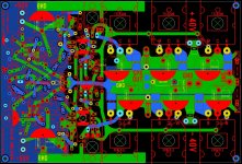
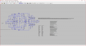
Yes, I checked it. The pcb layout corresponds to this schematic.
Regarding different power consumption on rails. I replaced Q16, Q17 transistors and nothing has changed. Turn off whistle sound only appears when 25 Ohm driver's bias R22, R23 resistors are used. DC offset disbalance during operation and I guess dc spike during turn off is happening because of negative side OP transistors (or one of them) consume more current and thus bias little higher than opposite half of transistors.
Last edited:
Btw, frontend psu LEDs have 1.5V drop, I don't know why after change R5, R6 to 9.1K was 1.38V, perhaps just after the start. So, as with R5, R6 11K and with 9.1K LEDs current is 1.5V.
When I replaced Q16, Q17 and checked the pcb for DC offset without mounting it on heatsink DC offset wasn't stable. After assambling it all together for uknown reasons dc offset is stable now and varies in range -5mV+25mV, but mostly -5mV+5mV with input bias current 4mA across emitter resistors. However, power rails consumption disballance still remains when turn off the amp. Amp start now with high DC offset disballance like +200+300mV when cold and from -60mV when hot and equalizes itself to zero.
Also after this mod, again for unknown reasons, the oscillation in 5mV deflection range is on the scope again with the same compensation as before.
Front end voltage is stable now, as I can see, and is dropping proportionaly with power rail voltages due to light bulb power limitation, keeping 10V difference between both.
R10, R11 voltage drop is from 18.7 to 19.6V. VAS bias current across R15, R14 - 240mV with 4mA input bias across R3, R5
Last edited:
Output bias, with maximum 10K set pot, is 120-135mA depending on heatsink temperature. In this case, I think it worth to increase Vbe multiplier resistors R37, R38 to 100 Ohms.
On the positive (sorry, my mistake, this is positive side with higher power consumption, not negative side) triple side with more consumption power rail one transistor has 8mA more bias current than other two, if this is somehow could be related with higher power consumption level.
On the positive (sorry, my mistake, this is positive side with higher power consumption, not negative side) triple side with more consumption power rail one transistor has 8mA more bias current than other two, if this is somehow could be related with higher power consumption level.
Last edited:
If your setting is with the light globe protection what you propose is taking a risk with a high a setting as 135 ma if you connect to the mains.
If you can now adjust that setting you should reduce it to a few ma per transistor for the next step - where you could use you variac to connect to the mains to see what upward adjustment is feasible.
If you can now adjust that setting you should reduce it to a few ma per transistor for the next step - where you could use you variac to connect to the mains to see what upward adjustment is feasible.
Last edited:
I didn't set such high bias current. It was done by itself with 4mA input bias and 24mA VAS bias. OP bias pot is at maximum position - 10K value. I reduced Vbe multiplier resistors to 36 Ohm to receive 77mA while heatsink is cold.
Simulation in my case lies about bias current and stability.
To use variac I need to put power resistor in series with variac secondary and measure the V drop on it? I have only secondary winding voltmeter in my variac.
Tried even 100p compensation at Q16, Q17 without success. Will try from base of first VAS tr-r to collector of second VAS tr-r later.
When I tried to play music, DC disbalance returned. I had to set the DC offset in a way it starts with -165mV and during normal listening level goes to +70mV.
The DC offset issue of this amp the most visible when it reproduces a low frequency signal with speaker cone moving (subwoofer test) in different frequency, the more the cone moves, more DC offset appears on out up to 1.5V rapid spikes
I think OP tr-rs are responsible for this. However I matched them for hfe and vbe before. Only one of them shows 7-8 higher bias current, others within 1-2mA range.
Output bias, with maximum 10K set pot, is 120-135mA depending on heatsink temperature. In this case, I think it worth to increase Vbe multiplier resistors R37, R38 to 100 Ohms.
On the positive (sorry, my mistake, this is positive side with higher power consumption, not negative side) triple side with more consumption power rail one transistor has 8mA more bias current than other two, if this is somehow could be related with higher power consumption level.
The 8 m.a. difference you have between opposites will be due to the settings of R8 and R9.
In simulations getting the values to minimise dc offset is an iterative and finnicky process. This may be harder to do in reality if you have two adjustments. At one stage I suggested making one of these a fixed value resistor to allow the balance adjustment to be made with one trim pot.
As you propose increase R37 and R38 to 100R. With the vbe trim at 10k and you need to get the conduction of the output stage down from 120-135 ma.
One assumes this is the total Iq not per transistor and that each of those in the output half is drawing current in equal shares. Is this what is happening?
No, difference with one transistor only, other 5 has almost the same bias. There is no problem in setting zero offset, much easier than in simulation. If I would have one trimpot I won't be able to change the bias.
Tried to increase R37, R38 to 100R, but it increased the bias even further, I lowered them to 36 Ohm. When heatsink was hot one transistor bias I measured was 13.5mV or 135mA, so per transistor.
Ideally, all the transistor shall draw the current equaly between each other. I matched them at 1A current, as I remember. During the music play with current draw spikes of more than 1A transistors could behave differently as unmatched in this current draw range. Perhaps it would be better to match them at 3-4A current.
No, difference with one transistor only, other 5 has almost the same bias. There is no problem in setting zero offset, much easier than in simulation. If I would have one trimpot I won't be able to change the bias.
Tried to increase R37, R38 to 100R, but it increased the bias even further, I lowered them to 36 Ohm. When heatsink was hot one transistor bias I measured was 13.5mV or 135mA, so per transistor.
Ideally, all the transistor shall draw the current equaly between each other. I matched them at 1A current, as I remember. During the music play with current draw spikes of more than 1A transistors could behave differently as unmatched in this current draw range. Perhaps it would be better to match them at 3-4A current.
When you include the driver stage with the outputs in the power section the demand for current is over half an ampere.
Charge carriers in a transistor whether electrons or holes original from the emitter. Most of these are attracted to the collector and the small amount flowing to the base has a resistor in series with the emitter diode.
The diode is not linear the resistor is and most of the voltage drop across the series combination will be due to the resistor.
The idea is the voltage drop across the resistor will swamp the effects of the base to emitter diode. This approach is known as base swamping.
This does have some limiting effects on hf which may not be a bad thing if a circuit is unstable -so within limits it can serve dual purposes.
As far as matching currents at 3-4 A is concerned if you have matched the devices at lower currents that step is not necessary.
However that still leaves the door open as to the flow between the emitter and collector which depends on the choice of emitter resistor value.
Btw, frontend psu LEDs have 1.5V drop, I don't know why after change R5, R6 to 9.1K was 1.38V, perhaps just after the start. So, as with R5, R6 11K and with 9.1K LEDs current is 1.5V.
Still mean that you redused current feed thru resistors at the same time and that R5 and R6 should bee further redused.
For the amp circ it seems like you are looking for a contact fait at the same time as dc ofset varies so much as you type her.
Yes so do i !I admire your persistence...
it's advised to match output devices in the current range they will be used in the circuit. Seems like for 100W output the current passes though every OP device is 1A?
I don't mind to use 0.2R emitter resistors. By now only 0.1R available in my disposal, I'll buy 0.2R later.
Maybe such high DC offset spikes are related with speaker coil? When the speaker cone moves it changes the DC resistance of the coil which affect the amplifier load and thus DC offset. This is partialy confirmed with high OP bias setting, when DC offset was stable while stable was amplifier load and relativly high current consumption. Maybe I should stress test the amp with dummy load (which will be stable in load). Does Mr. Self or Mr. Cordell say about it in the books?
How to culculate a minimum load for this amp circuit? Can I use 2.5 Ohm subwoofer with it?
Do you mean there could be a contact failure in the pcb or psu? I'm 90% sure that power rails contacts are firm and reliable, OP tr-rs soldered well, but I will check.For the amp circ it seems like you are looking for a contact fait at the same time as dc ofset varies so much as you type her.
Last edited:
Max power for output transistors when half available voltage at output.Maybe such high DC offset spikes are related with speaker coil? When the speaker cone moves it changes the DC resistance of the coil which affect the amplifier load and thus DC offset. This is partialy confirmed with high OP bias setting, when DC offset was stable while stable was amplifier load and relativly high current consumption. Maybe I should stress test the amp with dummy load (which will be stable in load). Does Mr. Self or Mr. Cordell say about it in the books?
How to culculate a minimum load for this amp circuit? Can I use 2.5 Ohm subwoofer with it?
Do you mean there could be a contact failure in the pcb or psu? I'm 90% sure that power rails contacts are firm and reliable, OP tr-rs soldered well, but I will check.
Yea somthing like a contact fault, but can bee almoust anywhere, even local oscillation may happen in som designs measures like dc with a multimeter...
What circuit are you using for output bias controll ?
Remember resistors in series with collector then basis output stage. This common mode rejection, termal tracking, Vas stage current variation suppression stage...... Does a lot if somthing like invisible jobs, but we like a "clear steady window" here the possibility to track bouth output and predriver. wariation in resistor values when voltage division is the same wil give different termal tracking.
So bee shore this picup nedle has so close to 2g at any time as possible may bee quite a task, but not always the goal 😉
another question is how muc your current sorces may wary ... ?
How abt a design using low noise 6.2V zener with simple filtering as reference for current sorces ?
Have you tryed too fast read som of the design treads that also wil give light to som of your truble.
Make it fun dig deeper !
These are 15A 150W 230V transistors, there are plenty of SOA left for them.
There is the oscillation, I found it at input emitter resistors and feedback resistors. Maybe somewhere else also.
I'm using current Vbe multiplier circuit for OP bias control. Q1, Q20 are bolted on top of OP tr-rs. Later I plan to use some SOT23 transistors for Vbe multiplier glued to collector leads of OP for better thermal tracking.
Do you mean 'resistors in series with collector' after VAS? Actualy at pcb I'm using 2.2R like in this sim, however simulation dosn't show they change the behaviour of the amp, I thought they can be omitted.There shouldn't be any variation in these resistor values, they are 1% tolerance 50 or 100 ppm. Also simulation shows VAS bias current for R15, R14 19mA, but I have 24mA. Maybe models of input transistors have too low beta, than I'm using?
How do I know how much my current sources may vary? To measure input cascodes base voltage during heavy loads if it sags? Previously Ian simulated thermal tracking of these current sources and found they have almost perfect thermal tracking in this circuit. I wrote you before about it exactly in his words.
Does there any low noise zeners exist? I don't understand the schematic fully, what is the reference for current sources in this schematic, D2, D1 or R10, R11? Btw, I'm using TL431 instead of zeners in this circuit.
I think the trouble here is to find out proper compensation method, but first I have to make new pcb for this SE schematic, as every layout requires its own compensation places and values. I almost done it, still left to refine it, remove some drc errors. I can show it for basic estimate.
I don't know any CFA design threads. I've read before SSA thread, but it wasn't about design.
Attachments
Last edited:
Two points - first the emitter resistor has a similar swamping effect on the base emitter diode resistance.
You might find an increase to 0.22R is not enough and you may have to experiment with higher values until you can get other problems sorted. One way to do this would be to buy some 1 watt 1R Carbon resistors and twist the leads of 4 of these together at both ends to make a temporary composite one of 0.25R.
Then if the need arises you can increase the composite value to 0.33R by snipping the lead of one of these and 0.5R by snipping the lead of a second one.
R Dijk's mention re Constant Current Sources prompts me to refer you to an article by Walt Jung on this subject where various types are considered. I have illustrated Jung's approach to the two transistor type which includes an additional resistor to ensure stability. For a fuller explanation you can follow the link at the top.
Attachments

These are 15A 150W 230V transistors, there are plenty of SOA left for them.
There is the oscillation, I found it at input emitter resistors and feedback resistors. Maybe somewhere else also.
I'm using current Vbe multiplier circuit for OP bias control. Q1, Q20 are bolted on top of OP tr-rs. Later I plan to use some SOT23 transistors for Vbe multiplier glued to collector leads of OP for better thermal tracking.
Do you mean 'resistors in series with collector' after VAS? Actualy at pcb I'm using 2.2R like in this sim, however simulation dosn't show they change the behaviour of the amp, I thought they can be omitted.There shouldn't be any variation in these resistor values, they are 1% tolerance 50 or 100 ppm. Also simulation shows VAS bias current for R15, R14 19mA, but I have 24mA. Maybe models of input transistors have too low beta, than I'm using?
How do I know how much my current sources may vary? To measure input cascodes base voltage during heavy loads if it sags? Previously Ian simulated thermal tracking of these current sources and found they have almost perfect thermal tracking in this circuit. I wrote you before about it exactly in his words.
Does there any low noise zeners exist? I don't understand the schematic fully, what is the reference for current sources in this schematic, D2, D1 or R10, R11? Btw, I'm using TL431 instead of zeners in this circuit.
I think the trouble here is to find out proper compensation method, but first I have to make new pcb for this SE schematic, as every layout requires its own compensation places and values. I almost done it, still left to refine it, remove some drc errors. I can show it for basic estimate.
I don't know any CFA design threads. I've read before SSA thread, but it wasn't about design.
Notice the smal changes and how muct it affects frequency responce.....
Pleace notice it is NOT renamed.
Attachments
Yes, very big difference from compensation capacitors placing change. R36, R39 have very little effect on frequency responce.
Why have you added C13 and changed R37, R38?
Why do you think there is such high discrepancy with my measurement results and simulation?
Tnx.
Why have you added C13 and changed R37, R38?
Why do you think there is such high discrepancy with my measurement results and simulation?
Tnx.
Last edited:
Yes, very big difference from compensation capacitors placing change. R36, R39 have very little effect on frequency responce.
Why have you added C13 and changed R37, R38?
Why do you think there is such high discrepancy with my measurement results and simulation?
Tnx.
The placing of compenssation was my point, and has the same placement as the first i showed when you did not get it stable.....
Whatever ... C9 and C12 now has the correct placement.
I added C13 to avoid anny discrapency between C3 and C5. and the possible influence on bias and freq induced dc/bias if C3 is not equal to C5 and R17 is not extactly R16
I belive its enough with 2 point measurment, they also measures inviroment.
I changed R37 R38 to giv the it more sensitivity to temp cause two diodes are removed to avoid unwanted temprature (read bias) swings due to termal delays and multiple measuringpoints. here R37 R38 may bee high.
Yes, very big difference from compensation capacitors placing change. R36, R39 have very little effect on frequency responce.
Why have you added C13 and changed R37, R38?
Why do you think there is such high discrepancy with my measurement results and simulation?
Tnx.
The simulation in post 773 shows that at -180 degrees where the gain margin needs to be below this one shows the gain as 5dB so there is no stability margin.
That in post in post 775 is somewhat better since there is some gain margin of - 6dB and a phase margin of -32 degrees.
One of the problems in approach common to both is the strategy of adding compensation capacitors in two circuit locations.
The notion of a single dominant pole will be compromised if the main choice is less than 10 times greater than any others.
I added C13 to avoid anny discrapency between C3 and C5. and the possible influence on bias and freq induced dc/bias if C3 is not equal to C5 and R17 is not extactly R16
I changed R37 R38 to giv the it more sensitivity to temp cause two diodes are removed to avoid unwanted temprature (read bias) swings due to termal delays and multiple measuringpoints. here R37 R38 may bee high.
Thanks for your clarification. I missed that you removed the diodes, but then there are 3 resistors in series. if so, can only one trimpot suffices?
Just noticed you shifted C13 from VAS collectors and reduced C20. Will try all on board.
- Home
- Amplifiers
- Solid State
- One of the Top Solid-State CFA amp design