Hmm, are you looking at how the amp is wired vs the recommended use as shown by THAT? Maybe I am dense, please show me if I am not seeing this via a diagram. But according to amp schematic +/- Diff input are connected to Vbe multiplier to handle bias. The +/- sense pins (normally tied to output via 10uF cap) is *not* connected to output but instead are tied together and actually are now the input audio signal. Yes, it goes through a 10K but that's just like an input series resistor (not in feedback path), so where's the feedback? It's the "input" now not connected to the output at all.
Edit: ok, I think I see what you mean now after studying it carefully. The 10k from each out to the -Cin is the feedback?
Edit: ok, I think I see what you mean now after studying it carefully. The 10k from each out to the -Cin is the feedback?
Last edited:
Hmm, are you looking at how the amp is wired vs the recommended use as shown by THAT? Maybe I am dense, please show me if I am not seeing this via a diagram. But according to amp schematic +/- Diff input are connected to Vbe multiplier to handle bias. The +/- sense pins (normally tied to output via 10uF cap) is *not* connected to output but instead are tied together and actually are now the input audio signal. Yes, it goes through a 10K but that's just like an input series resistor (not in feedback path), so where's the feedback? It's the "input" now not connected to the output at all.
Edit: ok, I think I see what you mean now after studying it carefully. The 10k from each out to the -Cin is the feedback?
Right - those two 10K's are the ones.
The gain of each inverting amp is 2x or 6dB. In the fig 2 (post #80) the 10k between Dout- and Din+ in combination with the 5k input resistor appear to set this gain. This may also be why the data sheet says the device should be driven from a low impedance source. Another pair of feedback loops.
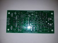
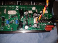
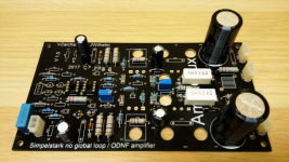
The Einbahnstark input for the NS series amplifiers is running nicely. Here's a test run with +/- 63V supplies. The supply is sagging quite a bit under load leading to 150W RMS output. i'm finding the input is running warmer than I would like so I'm going to retest it at a more civilized voltage.
Attachments
Hi Valery.
I have found my papers with mods on NAD S300.
As You see it is important to isolate speaker output from feedback loop to prewent any intrusion of inductions in voice coils and crossowers and RF signals recieved with speaker cables. And without global feedback loop You need larger idling current to owercome power transistor nonlinearitys at low currents.Optimal local feedback wold be 9-12dB and owerall 350mA idling current(2 transistors)wood be enough.
As Nelson Pass says 10dB feedback and first watt-350mA idling current.
Look also my post #20 at CF-FET V2.0(SMD) and tnt-audio.com/Solid State/Put a tiger into your amp.From interest ware also schematics of ONKYO A9911,9711,927LTD.
Cheers,Bozo
Attachments
Why using Laterals as drivers and also the large mosfets load the previous stage badly though increasing the distortion. Can you try using ksa1381 3503sFinally - not as sophisticated and accurate as the previous one, but a rather simple one and still promising in terms of the way it's going to sound.
Self-biasing IPS, trimmers for OPS offset and bias settings.
Hi All,
As many times discussed, feedback is inevitable, being present everywhere around us. We also use it every time we design an audio amplifier.
Important point – the way we use it.
No doubt, it’s possible to design a good (or not so good) amplifier with both global NFB loop in place or no global loop at all – in this case, several local NFBs are utilized for controlling important parameters.
After testing / auditioning different designs throughout the recent years, I come to conclusion I like the way the good no-global-loop amplifiers sound. Those amplifiers are well-known in the world of vacuum tubes for decades. However, my focus are solid-state amplifiers and hybrids, designed with series of local feedback (preferably covering a single stage) loops in mind. Damir and other members presented a number of excellent works in this area.
In this thread, I’d like to share my experience in designing an important part of any amplifier – the front-end, providing all the voltage gain – utilizing only local feedback loops.
Picture 1 illustrates possible arrangement in principle.
Input stage (transconductance, Gm = 0.5 mA/V) is a heavily degenerated CE circuit – that’s where the most of distortion is born, however at the volume of degeneration used, it’s low enough for the purpose.
Emitter degeneration provides a series-series feedback, providing the desired transconductance ratio and linearizing the transfer function.
2-nd stage is a high-precision cascaded current mirror with current gain of around 2x – highly linear mirroring with a little bit of gain.
Finally – passive transimpedance conversion – resistor load – also very linear, assuming both the output impedance of the current mirror and input impedance of the next stage are high enough.
To satisfy the latter assumption, we have to use a high-quality unity-gain buffer between this resistor and the OPS, as OPS’s input impedance, although it can be rather high, is normally more (especially in case of MOSFET drivers) or less capacitive and rather modulated (especially in case of BJT arrangement).
Small value capacitor provides minimal correction, eliminating possible frequency response artifacts above 1MHz.
It's easy to arrange a balanced input or a fully balanced architecture here - no global loops make it beautiful (just servo needs a bit of redesign).
Picture 2 illustrates practical implementation of the above ideas.
The circuit demonstrates pretty good performance – although, I’m presenting simulated results here, I have measured and listened a rather close (a bit less sophisticated) design, showing similar results and sounding just great.
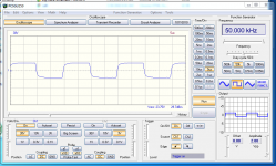
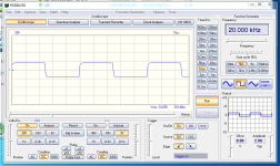
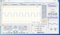
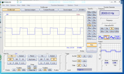
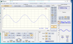
Pictures 3, 4, 5 and 6 illustrate:
- Spectrum at 1 KHz (20V RMS0;
- Spectrum at 20 KHz (20V RMS);
- Square wave response at 20KHz (60Vpp);
- Frequency response.
Harmonics 2, 3 and very little bit of 5. Looks like a spectrum profile from the vacuum pentode ��
There may be many different implementations of the stages, including jFETs at the input, folded cascode instead of current mirror, simpler unity gain buffer, etc.
In terms of OPS selection – it must be a low-distortion one. Class A / AB (well-designed CFP, properly biased EF, MOSFET outputs, some error-correction options, non-switching arrangements, etc.).
I used NS-OPS, showing THD < 0.05% open loop throughout the whole audio bandwidth.
What do you think?
Cheers,
Valery
P.S. A simpler no-global-loop headphone amp design is presented here:
Aureaux high-quality no-global-loop headphone amp
Valery how is bias is being set on the Einbahnstark.
Why using Laterals as drivers and also the large mosfets load the previous stage badly though increasing the distortion. Can you try using ksa1381 3503s
Laterals as drivers are very good. Mid-power oned - like 2SK216/2SJ79 - may fit even better, however, those are obsolete - rather hard to find.
You would have a "bad VAS loading" problem with the HexFETs here, but laterals are very different - input capacitance is not that high, plus it's linear enough (in terms of the input swing at MOSFET's gate).
ksa1381 c3503 will not give the result good enough because of the driver stage input impedance modulation.
Valery how is bias is being set on the Einbahnstark.
Schematic in post #1 is the front-end only (no OPS showed). The output you see there is a unity gain class A buffer stage for isolating the VAS stage from the OPS input impedance modulation.
Solving the same issue, as mentioned in the post above (with regard to laterals), but in a more sophisticated way.
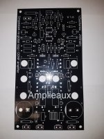
no GNF should sound good now even with lower Output impedance it believe it will sound even better. If you can push the output impedance to another digit down it will be very nice.The first prototype build progress so far
Waiting for some components to arrive.
I think that Jeff will sent this new amplifier for test soon.
This is in the package. Valery will send you the latfets for it though, I think my stock is fake.
This is in the package. Valery will send you the latfets for it though, I think my stock is fake.
Fake parts all over the world

- Home
- Amplifiers
- Solid State
- No-global-loop amplification