Got a couple of queries and comments bit will post later
We've had an Internet outage all day and I'm sending this from my phone. Can't be bothered to poke at it anymore. Will post when I've got a proper keyboard to use. Yeh I know I could connect a keyboard to my phone but finding the cables etc. is just to much hassle. Sorry.
We've had an Internet outage all day and I'm sending this from my phone. Can't be bothered to poke at it anymore. Will post when I've got a proper keyboard to use. Yeh I know I could connect a keyboard to my phone but finding the cables etc. is just to much hassle. Sorry.
Ahh Internet back up!
I meant simple in the sense that the original AEM6000 is a novel, but straightforward, assembly of standard circuit blocks. You can see the broad outline of what the designer was trying to achieve at a glance. Cordells amplifier with CMCL and error feedforward - now thats complicated! It would have taken me forever to deconstruct that without guidance. Remember too that I was a career scientist and we used simple as a compliment not in any pejorative sense.
Returning to my original question. The collector current of Q14 has two components; one is fixed by the current source and the other comes from Q15 via R36. Now Q15 can both service its constant current load and provide an extra, arbitrary, current to Q14 because its base emitter voltage is not fixed. Thus in addition to supplying their respective current sources Q14 and Q15 can supply each other with any arbitrary current, via R36, in exactly the same way as in your original proposal. Is it possible that you've found a deep metastable state, but not the global stable state? Anyway I'd be grateful if you'd explain the flaw in my reasoning - had a drink or two before I proposed it.
Q14 and Q15 now each have two collector loads in parallel - each other and their respective current sources so the total impedance will be lower than that of the Stochino style current mirror. This means that the open loop gain will be lower and the distortion higher - assuming stability. Important if you're now chasing tenths of a ppm!
I'm not entirely sure what you mean by a Stochino current mirror. Is it perhaps this:
I can't see a mechanism for the VAS transistors to be turned hard on. The servo loop keeps the current on both sides of the diff pair approximately equal with no error, so half the tail current is flowing down the mirror. It's collector is tied to its base, so that defines the collector voltage on that side of the mirror. Symmetry says the voltage on the other side will be reasonably close.
I think the simulation that'll show any problems will be the circuits response to a square wave input, as the fast transient will introduce significant servo errors.
Granted there's an additional collector load on the VAS in my one, but the Stochino circuit imposes an additional base load on the preceding stage, so it's probably swings and roundabouts.
It may be that a bulletproof method of stabilising the VAS current is with a couple of diodes and a series resistor as a clamp on the VAS base. Under normal conditions it wouldn't do anything, but if the base voltage goes too high it'll conduct a little and stabilise. The result of that would be poorer transient response.
An externally hosted image should be here but it was not working when we last tested it.
I can't see a mechanism for the VAS transistors to be turned hard on. The servo loop keeps the current on both sides of the diff pair approximately equal with no error, so half the tail current is flowing down the mirror. It's collector is tied to its base, so that defines the collector voltage on that side of the mirror. Symmetry says the voltage on the other side will be reasonably close.
I think the simulation that'll show any problems will be the circuits response to a square wave input, as the fast transient will introduce significant servo errors.
Granted there's an additional collector load on the VAS in my one, but the Stochino circuit imposes an additional base load on the preceding stage, so it's probably swings and roundabouts.
It may be that a bulletproof method of stabilising the VAS current is with a couple of diodes and a series resistor as a clamp on the VAS base. Under normal conditions it wouldn't do anything, but if the base voltage goes too high it'll conduct a little and stabilise. The result of that would be poorer transient response.
Yes thats the stochino circuit. The pairs of 2N2222As at the top and bottom centre are in fact current mirrors, the right hand ones program the current via the 22k 2W resistor and the left hand ones are the vas transistors proper.
Its the phrase "Symmetry says the voltage on the other side will be reasonably close." that encapsulates my worry. Remember the Randy Sloane amplifier that toasted so many transistors for its unwitting constructors did actually work for a few people. I think some method of limiting the vas current would be a wise idea - I'd probably use a transistor rather than a diode but it doesn't really matter. In the end I guess only a prototype will tell. If it does work reliably then you'll have the satisfaction of coming up with a novel configuration rather than using pre-existing schemes. I'd sprinkle a few diodes about like Stochino to stop the mirrors and vas from saturating.
Its the phrase "Symmetry says the voltage on the other side will be reasonably close." that encapsulates my worry. Remember the Randy Sloane amplifier that toasted so many transistors for its unwitting constructors did actually work for a few people. I think some method of limiting the vas current would be a wise idea - I'd probably use a transistor rather than a diode but it doesn't really matter. In the end I guess only a prototype will tell. If it does work reliably then you'll have the satisfaction of coming up with a novel configuration rather than using pre-existing schemes. I'd sprinkle a few diodes about like Stochino to stop the mirrors and vas from saturating.
Modifying the current mirrors will give you the best of both worlds - guaranteed dc stability plus use of your own vas configuration. The current mirror mods add a helper transistor and a 47k differential load across the mirror collectors. If the loss of olg is a worry you could make it up elsewhere.
Ah well at least I've got the excuse that I' getting on a bit. I agree that your proposed arrangement will be dc stable. My post #34 summed it up. I had indeed missed considering a feedback loop by not considering the key effect of connecting the vas current sources back to the current sources of the previous stage. Very neat. Are you going to post a "final" schematic before committing to pcb fabrication? I must admit that I usually hand make prototypes to spare me the expense of junking a few pcbs if I get it wrong. I always remember the first batch of pcbs I had done:- I asked how much one prototype would cost and was told £200; then I asked how much a batch of 32 would cost - you guessed it - £200!
I've done a fair bit of RFIC design for work. That's both good and bad. Good in that you get a lot of exposure to very low level circuit design techniques, bad in that everything really is matched very well on die, and when you're designing stuff off-chip you've got to remember that's not always the case.
Oh, and a prototype run for the fairly pedestrian 0.18um process I was working in: $50k. Makes for rather more stress in taping out than I'm comfortable with.
I'll post a schematic of where I'm at later in the day when I'm at my computer. As for layout I'm splitting the whole thing into 2 PCBs: one for the latFETs, with their decoupling, emitter resistors, and gate components (plus some power supply stuff in this case) and a second board for the low-power stuff. My rationale is that I can try different topologies by building a 3cm x 8cm PCB rather than a much bigger board. Also I can re-use the same low power board for a dual-driver 150W version, or even a bigger triple driver 220W version.
Are you going to use drivers for the lafets? That and multiple lafets would lead to quite a drop in output stage distortion. I've used the two pcb implementation as well; very useful for experimenting but not quite so aesthetically pleasing for a "keeper" amp. Will really be out of the loop for the next few days - off to welcome grandchild no. 6 to the world tomorrow.
Hi Suzyj,
Wondering if you've ever considered building Bob Cordell's old MOSFET amp, even without the error correction:
CordellAudio.com - A MOSFET Power Amplifier with Error Correction
Or the APT 1:
http://www.diyaudio.com/forums/solid-state/70261-apt-1-power-amp-undeservedly-forgotten.html
Wondering if you've ever considered building Bob Cordell's old MOSFET amp, even without the error correction:
CordellAudio.com - A MOSFET Power Amplifier with Error Correction
Or the APT 1:
http://www.diyaudio.com/forums/solid-state/70261-apt-1-power-amp-undeservedly-forgotten.html
Are you going to use drivers for the lafets? That and multiple lafets would lead to quite a drop in output stage distortion. I've used the two pcb implementation as well; very useful for experimenting but not quite so aesthetically pleasing for a "keeper" amp. Will really be out of the loop for the next few days - off to welcome grandchild no. 6 to the world tomorrow.
I've done some simulations with emitter followers and see no improvement in 10KHz distortion level. I'm not convinced that the input capacitance of the lateral mosfets really warrant the driver stage - as long as I've got a healthy VAS current I've got ample drive at 10KHz. Certainly the following circuit simulates 0.0005% THD at 10KHz, 50W, 8R load, and 0.00005% at 1KHz.
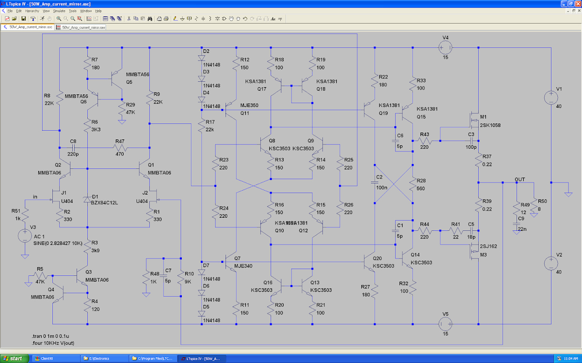
Key to this is working on the loop stability so that I can push the gain down. Of course this is just the sort of optimisation that has to be repeated with the real amplifier. I found the amp with driver much harder to stabilise.
Hi Suzyj,
Wondering if you've ever considered building Bob Cordell's old MOSFET amp, even without the error correction:
CordellAudio.com - A MOSFET Power Amplifier with Error Correction
Or the APT 1:
http://www.diyaudio.com/forums/solid-state/70261-apt-1-power-amp-undeservedly-forgotten.html
That Bob Cordell linearised output stage is very cool. I was up really late last night trying to get it to simulate with no joy at all.
If you're going to the extent of using drivers for the mosfets, and higher supply rails for the frontend, id probably be inclined to say using cascodes is simpler. Split pole compensation is also really worth a look.
Here's my current sim plaything...
Interesting, similar to something that I've been playing with but mine is without most of those cascodes. Did you consider JFETs for the diff pair?
Didn't consider JFETs because sourcing them is a hassle. The CFP in the input LTP is also guilding the lily a bit - i could find no difference in THD results with or without this. I'll probably lay out the PCB to accomodate it anyway, as it can be left off by installing 0 ohm jumpers for R33/34.
Split pole compensation is definitely worth using. Easy to get THD at 10KHz way down from usual using this.
Cascoding is a nice tool too, and makes the type of medium power transistor used in this stage much less critical. As suitable "video driver" type transistors are dying out, its good to see that you can get good performance using MJE340/350 by simply using a cascode arrangement
Didn't consider JFETs because sourcing them is a hassle. The CFP in the input LTP is also guilding the lily a bit - i could find no difference in THD results with or without this. I'll probably lay out the PCB to accomodate it anyway, as it can be left off by installing 0 ohm jumpers for R33/34.
Split pole compensation is definitely worth using. Easy to get THD at 10KHz way down from usual using this.
Cascoding is a nice tool too, and makes the type of medium power transistor used in this stage much less critical. As suitable "video driver" type transistors are dying out, its good to see that you can get good performance using MJE340/350 by simply using a cascode arrangement
Did you consider the BF862 for the FETs?
True about the cascode, still the complexity of higher supplies is not for me.
I think you mentioned in this thread about the discussions on current source stability
but you don't have the extra resistor in your 2T is that just a detail to come?
Did you consider the BF862 for the FETs?
It was more a case of "Do I have them in my parts collection already ?"
")
True about the cascode, still the complexity of higher supplies is not for me.
Not as complex as you'd think actually. I'm using a 120VA 28-0-28 EI transformer I salvaged from somewhere to power this, and to get the extra supplies i'm using a voltage doubler followed by simple zener regulator. This can quite comfortably manage 100mA and is plenty for the frontend.
I think you mentioned in this thread about the discussions on current source stability but you don't have the extra resistor in your 2T is that just a detail to come?
True, overlooked it. Whether its needed seems to vary! I might even change this arrangement and use another BAV99 as the reference.
Attachments
Hello everybody,
my bunch of PCBs arrived from PCBWay, and i am strarting now to build up the amplifiers. Thanks again for that wonderful design to Suzy Jackson.
So, what are the hints and tricks to make this beautiful amps successfully work.All parts (Melfs, capacitors, SMD transistors, driver and powe transistors are already available. The pcbs are double layers with 2 oz (70µ) copper. As far as i know, Suzy uses 3 oz PCBs.
Any comments to that project???
Best regards
Gunni
Hi Gunni,
i had built the PCB that was bought from you, and it works and it sounds ok but i can not adjust the quiescent current according to Suzy recommendation which is 100ma per transistor, i have adjusted RV2 to max and the highest i can get is 4.4mV from .22R resistor which is only around 20mA each transistor. any suggestion how to fix the problem?
regards,
mj777
- Status
- This old topic is closed. If you want to reopen this topic, contact a moderator using the "Report Post" button.
- Home
- Amplifiers
- Solid State
- AEM 6000 ready to build