A circuit with only a single gain stage gives you very little spare loop gain for NFB, and small amounts of NFB rather tend to make matters worse. 40+ dB, now that's something to work with. Practical ones tend to use a second gain stage for this very reason, JLH included.
You could try and "cheat" by using an LM338 for the CCS, much like in the application circuit suggested in its datasheet. Just be aware that you can't put the output transistor on the same heatsink w/o providing insulation for one of them.
Quiescent current limits maximum negative voltage swing depending on load. Basically the output transistor can only "push", the CCS is the only one to "pull". Hence the current drawn from the load at maximum negative output needs to be smaller than quiescent current.
A push-pull output stage neatly doubles current output at same Iq, i.e. 4 times the power in Class A.
As far as complexity goes, more is definitely more, it just becomes ever harder to make work. Any amplifier can be seen as a tradeoff between complexity, power consumption and performance. People in DIY land like Class A amps because they can give good performance with a handful of transistors, even if the beefy power supply and cooling required drive up cost nowadays. A good AB amps requires some more effort, and if you really need a power miser, then you may have to resort to ICs with hundreds of active parts in them.
A circuit with only a single gain stage gives you very little spare loop gain for NFB, and small amounts of NFB rather tend to make matters worse. 40+ dB, now that's something to work with. Practical ones tend to use a second gain stage for this very reason, JLH included.
You could try and "cheat" by using an LM338 for the CCS, much like in the application circuit suggested in its datasheet. Just be aware that you can't put the output transistor on the same heatsink w/o providing insulation for one of them.
Thanks sgrossklass for your advice.
I have decided to 'cheat' and use an ne5534 low noise op-amp as the vas, this is capable of driving the bd139. I have also put a 75ma CCS from the bd139 emitter to ground ( using an lm317) to improve performance. I also tried using an lm350 as a 1.2A CCS for the output stage, I could not get this to work, the current limit kept operating on my bench PSU, everything else worked with the lm350 removed, note that feedback was taken from the emitter of the output transistor back to the opamp, all the wiring was checked and there were no shorts. Could it be a bad lm350 or perhaps HF instability, I've heard that, that can sometimes happen when using these regulators as current sources.
I am going to make a 2 transistor CCS with another tip3055 and a bd139, and see how that goes.
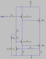
A proper schematic!
Joy of joy, I have found a schematic capture app for my android tablet.
Attached is the latest draught of the amplifier, haven't built this yet but planning on tomorrow.
Again any constructive criticism is very welcome.
Joy of joy, I have found a schematic capture app for my android tablet.
Attached is the latest draught of the amplifier, haven't built this yet but planning on tomorrow.
Again any constructive criticism is very welcome.
Attachments
Plus:
Include ~470R of series resistance and ~330 pF to ground at the input for better EMI suppression.
Should you find insufficient supply hum rejection, use a somewhat more elaborate filtered voltage divider setup (e.g. 10k/(10k||22µ) tapped via 47k).
R3/R4 are on the highish side, which may result in ultrasonic peaking due to opamp input capacitance (noise and added distortion would be insignificant here). Either include a parallel cap for R4 (~30-ish pF for a ballpark figure) or reduce values by maybe a factor of 5, with a 'lytic (or two polar ones back-to-back) for C3.
'C1' is used twice.
I hope you're well-stocked in terms of heatsinks and/or insulating washers/pads.
The basic design seems sensible though, it looks like something that should work well within its limits. At these lowish supplies, do not entirely discount oldschool power transistors. BD243C or TIP41C may also be worth a shot if you have some floating around.
BTW, I realise that draught and draft are pronounced the same and derive from some kind of 'drawing' or another, but for things related to sketches, you want draft instead.")
Include ~470R of series resistance and ~330 pF to ground at the input for better EMI suppression.
Should you find insufficient supply hum rejection, use a somewhat more elaborate filtered voltage divider setup (e.g. 10k/(10k||22µ) tapped via 47k).
R3/R4 are on the highish side, which may result in ultrasonic peaking due to opamp input capacitance (noise and added distortion would be insignificant here). Either include a parallel cap for R4 (~30-ish pF for a ballpark figure) or reduce values by maybe a factor of 5, with a 'lytic (or two polar ones back-to-back) for C3.
'C1' is used twice.
I hope you're well-stocked in terms of heatsinks and/or insulating washers/pads.
The basic design seems sensible though, it looks like something that should work well within its limits. At these lowish supplies, do not entirely discount oldschool power transistors. BD243C or TIP41C may also be worth a shot if you have some floating around.
BTW, I realise that draught and draft are pronounced the same and derive from some kind of 'drawing' or another, but for things related to sketches, you want draft instead.
Last edited:
On second thought, this doesn't seem right. It would have to be more like 0.33 pF.Either include a parallel cap for R4 (~30-ish pF for a ballpark figure)
Anyway, if you really want to keep feedback network divider ratio the same as far as possible, you can always add parallel caps to both R3 and R4 with their values inversely proportional to resistor values. So maybe 5 pF for R4 and 39 pF for R3. Opamp input capacitance tends to be in the 2-5 pF ballpark, and 39 pF should easily dominate it.
Thanks again jerluwoo and sgrossklass.
I have incorporated most of the suggestions. I have opted to scale down the feedback resistors ( 18k & 2k ), that seemed like the most straightforward thing to do.
I have also used TIP41 instead of TIP3055, I am intending to try a 2sc5200 as the output transistor, do I need to get another 2sc5200 for the CCS, as I'm only getting 1 2sc5200, if so I'll need to order another one.
I have nearly finished building a mono prototype. All the heavy current wiring has been done on terminal blocks, using 6 A flexible mains cable, with a star ground point.
Yes, I do have plenty of to220 mounting kits and silicon grease!
I have included the latest draft ( not draught )
I have incorporated most of the suggestions. I have opted to scale down the feedback resistors ( 18k & 2k ), that seemed like the most straightforward thing to do.
I have also used TIP41 instead of TIP3055, I am intending to try a 2sc5200 as the output transistor, do I need to get another 2sc5200 for the CCS, as I'm only getting 1 2sc5200, if so I'll need to order another one.
I have nearly finished building a mono prototype. All the heavy current wiring has been done on terminal blocks, using 6 A flexible mains cable, with a star ground point.
Yes, I do have plenty of to220 mounting kits and silicon grease!
I have included the latest draft ( not draught
)Attachments
Last edited:
Teething troubles
Today has been a bit of a nightmare, but hopefully an educational one!
I built the circuit as outlined in my last post and so far no joy, several transistors have sadly passed away in their service to the cause!
At first there was a problem with the VAS and driver section, these were built on the breadboard. The circuit was drawing excess current. The high power section was disengaged at this time to aid fault finding in the low power part of the circuit. This section was found to be drawing excess current too. I make systematic tests of voltages, there appeared to be a fault in the opamp and the driver transistor, the transistor was removed and tested, it had failed. The opamp and driver transistor where replaced and power reapplied carefully with current limit control, it was still drawing too much current. I checked the lm317 and the voltage across the 16 ohm resistor was a bit high, about 1v45 I think ( forgot to write it down ) I replaced the lm317 and the voltage on the 16 ohm resistor was lower but still not within spec, I'm now suspecting the lm317's are suspect ( they were bought from a Chinese eBay seller ) I replaced the CCS with a 200 ohm resistor and it worked fine. I had the same problem the other day trying to use an lm350 as a CCS in the output stage.
Having given up on the regulator based CCS, I went with the 200 ohm resistor and reconnected the output stage. Again the supply current was climbing way too high as I gradually increased the constant current level on my bench PS.
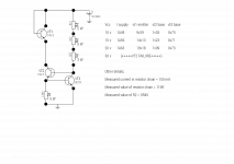
This time I disengaged the output section for fault finding. The output and CCS transistors were all found to have failed. ( note they had all tested as working prior to inclusion in the circuit ) I replaced them all and ran the output section disengaged with the base of the output transistor connected to +Vcc. Again the current limit was raised slowly, in fact I done it first with a maximum of 10 volts, then 15, then 20 and all was OK until I tried Vcc of 30 volts and the tip41 in the CCS failed. I have charted the testing of the output stage on the attached diagram. It seems that it was ok until Vcc was increased to 30 volts, on examination it was found that the faulty transistor had not been securely bolted to the heatsink and I'd forgotten to put heatsink compound on so looks like it overheated!
That's were I'm at now.
I am still unclear on what went wrong with the lm317 CCS and the failure of all the transistors first time round, maybe it was just bad components? I am wondering also if the tip41's are up to the task, the st data sheet does not have a safe operating area graph so I'm not sure whether we are getting into dangerous waters with this circuit and tip41 transistors. I will try one more time with the tip41 and ensure heatsink paste and a very tight fastening to the heatsink are made. But now I am tired and need to spend some time with my girls. Please share any thoughts regarding the CCS malfunction, it is still a bit of a mystery to me.
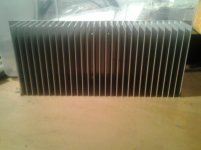
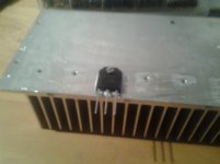
Also, I think that the heatsink is big enough, see attached pictures. I got it used for only 5.00 GBP, about 7.50 USD, so I don't actually know the °C per watt rating, but it was from a 350 watt audio amplifier.
EDIT: The bd139s have been run with no heatsinking and their max dissipation without h/sink is only 1.25 watts ( oops!!!! )
Today has been a bit of a nightmare, but hopefully an educational one!
I built the circuit as outlined in my last post and so far no joy, several transistors have sadly passed away in their service to the cause!
At first there was a problem with the VAS and driver section, these were built on the breadboard. The circuit was drawing excess current. The high power section was disengaged at this time to aid fault finding in the low power part of the circuit. This section was found to be drawing excess current too. I make systematic tests of voltages, there appeared to be a fault in the opamp and the driver transistor, the transistor was removed and tested, it had failed. The opamp and driver transistor where replaced and power reapplied carefully with current limit control, it was still drawing too much current. I checked the lm317 and the voltage across the 16 ohm resistor was a bit high, about 1v45 I think ( forgot to write it down
) I replaced the lm317 and the voltage on the 16 ohm resistor was lower but still not within spec, I'm now suspecting the lm317's are suspect ( they were bought from a Chinese eBay seller ) I replaced the CCS with a 200 ohm resistor and it worked fine. I had the same problem the other day trying to use an lm350 as a CCS in the output stage.Having given up on the regulator based CCS, I went with the 200 ohm resistor and reconnected the output stage. Again the supply current was climbing way too high as I gradually increased the constant current level on my bench PS.
This time I disengaged the output section for fault finding. The output and CCS transistors were all found to have failed. ( note they had all tested as working prior to inclusion in the circuit ) I replaced them all and ran the output section disengaged with the base of the output transistor connected to +Vcc. Again the current limit was raised slowly, in fact I done it first with a maximum of 10 volts, then 15, then 20 and all was OK until I tried Vcc of 30 volts and the tip41 in the CCS failed. I have charted the testing of the output stage on the attached diagram. It seems that it was ok until Vcc was increased to 30 volts, on examination it was found that the faulty transistor had not been securely bolted to the heatsink and I'd forgotten to put heatsink compound on so looks like it overheated!
That's were I'm at now.
I am still unclear on what went wrong with the lm317 CCS and the failure of all the transistors first time round, maybe it was just bad components? I am wondering also if the tip41's are up to the task, the st data sheet does not have a safe operating area graph so I'm not sure whether we are getting into dangerous waters with this circuit and tip41 transistors. I will try one more time with the tip41 and ensure heatsink paste and a very tight fastening to the heatsink are made. But now I am tired and need to spend some time with my girls. Please share any thoughts regarding the CCS malfunction, it is still a bit of a mystery to me.
Also, I think that the heatsink is big enough, see attached pictures. I got it used for only 5.00 GBP, about 7.50 USD, so I don't actually know the °C per watt rating, but it was from a 350 watt audio amplifier.
EDIT: The bd139s have been run with no heatsinking and their max dissipation without h/sink is only 1.25 watts ( oops!!!! )
Attachments
Last edited:
If you got all these parts from unknown china ebayer they could all well be junk. Your testing method for the tip41 ccs subjected it to close to 50 watts which would have probably killed a genuine part anyway. The fairchild datasheet shows derating down to 28 watts @ 100c and an soa @ 30V of 2A before derating, 933mA after, so dead transistor for your testing method @ 30V. They are just barely able to take the power at what would be the operating point of 15V @ 1.6A in a correctly working circuit. Reduce the current down to 1A to try and get it going first. Use of to247/to3p devices is recommended at a minimum to have any longevity, even having to220's at or slightly under there limit will still have a high probability of failure.
Thanks again Jerluwoo, you are right now that I think about it, its remarkable really that there wasn't any smoke!
Iam going back to the Tip 3055's, they were from a reliable source and they have much more headroom, also they are in the to3p case, which I believe is better able to transfer heat to the heatsink ( larger surface area I suppose. )
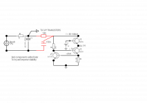
I have attached a draft of the latest proposed modifications,
Attachments
Update:
The to-3p insulation washers arrived today as well as some other parts that I ordered with a view to trying out alternate class a output stages.
I've attached the two tip 3055's to the big heatsink and put small heatsinks on the bd139's, nearly ready for a second trial run. As per jerluwoo's suggestion I'll start of at 1A standing current and see how it goes from there.
I have 2 2sk1058 n-mosfets, I wondered about trying these in the output stage, the CCS loaded driver should be able to push enough current to overcome the MOSFETs input capacitance. Anyone have any thoughts on that?
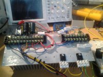
All of the output stage is wired up now, see attached photo.
Reckon it would sound good with this opamp:
LT1028 - Ultra Low Noise Precision High Speed Op Amps - Linear Technology
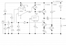
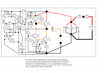
The second image is the output stage wiring diagram, with comments.
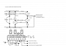
The third image is the driver stage, schematic and layout diagrams. I will build this today ( wed 11th ) after I have slept.
Reckon it would sound good with this opamp:
LT1028 - Ultra Low Noise Precision High Speed Op Amps - Linear Technology
The second image is the output stage wiring diagram, with comments.
The third image is the driver stage, schematic and layout diagrams. I will build this today ( wed 11th ) after I have slept.
Attachments

Last edited:
Changes I would make on the discrete section. Less overall current consumption and better noise performance.
Thanks again jerluwoo. I have already built my circuit this morning, just need to connect up the discrete driver / output stage to the opamp.
Your circuit is very smart it even uses less transistors!
2 questions: The 10R resistor between the opamp and the base of the driver transistor, is this a base stop resistor to improve AC stability?
What is the purpose of the 1K resistor?
Gordon.

The driver stage is acting really strange. See attached diagram.
DC voltages and currents kept changing when DVM probe applied to various points in the circuit. I suspect oscillations.
I was unable to locate my 100n ceramic capacitors for local decoupling, so the circuit was built without them. Later I added The red 10R resistor and 150n capacitor ( mylar or polyester ) which did tame the variations being caused by the meter probe.
I need to examine this circuit with the 'scope.
Do you think the odd behavior is due to parasitic oscillations?
?Remedy?
All the transistors have been tested and retested; All OK.
Attachments
The 10 ohm is to isolate the opamp from it's load and should be placed at the output pin on the opamp rather than at the base of the transistor. The 1k forms a low pass filter with the input capacitance of the transistor, it can help with high frequency issues.
As for the funny readings, oscillation is the primary suspect. Many believe a simple emitter follower is always stable but it doesn't really take much to turn it into an oscillator, Emitter followers as Colpitts oscillators | EDN If there is going to be a length of wire between opamp output and base of the driver transistor it may need a resistor at the base pin as well as opamp output.
As for the funny readings, oscillation is the primary suspect. Many believe a simple emitter follower is always stable but it doesn't really take much to turn it into an oscillator, Emitter followers as Colpitts oscillators | EDN If there is going to be a length of wire between opamp output and base of the driver transistor it may need a resistor at the base pin as well as opamp output.
The 10 ohm is to isolate the opamp from it's load and should be placed at the output pin on the opamp rather than at the base of the transistor. The 1k forms a low pass filter with the input capacitance of the transistor, it can help with high frequency issues.
As for the funny readings, oscillation is the primary suspect. Many believe a simple emitter follower is always stable but it doesn't really take much to turn it into an oscillator, Emitter followers as Colpitts oscillators | EDN If there is going to be a length of wire between opamp output and base of the driver transistor it may need a resistor at the base pin as well as opamp output.
Thanks jerluwoo,
I will try the base stop resistor at the base of the driver transistor. It was being fed by a long wire from the other channel of the bench supply ( the 5 v source ) so probably some inductance there. I will try a 1K ? resistor at the base of the bc547, also I might split the 3K9 into 2k + 2k with a bypass capacitor to ground like in your circuit.Also I will improve PS decoupling close to the section, an electro cap // ceramic.
If it still doesn't work well, I will try building your circuit.
What do you think of my idea of using two 2sk1058 N-Mosfets?
Thanks jerluwoo,
What do you think of my idea of using two 2sk1058 N-Mosfets?
The results will be nearly the same sound-wise as the dominant item here will be the opamp sound. Less power output due to the extra turn on voltage of the fets.
The results will be nearly the same sound-wise as the dominant item here will be the opamp sound. Less power output due to the extra turn on voltage of the fets.
Pretty much what I figured.
Having decided that your idea was too good to ignore, I've decided to go with it but with some slight variations. Any comments / criticisms are welcome, as always.
1. I have made provision for the idle current to be variable from ~ 700 to 1400mA with a 1K trim pot.
2. The error amplifier transistor in the CCS has been changed to a higher gain type, bc547 probably.
3. Star point wiring for power supply connections.
4. Additional local decoupling ( in red )
5. Zobel network across the output.
Attachments
I have built the modified version of jerluwoos driver / output stage and connected it up to the ne5534 VAS.
The quiescent current of both driver and output transistors were on the low side. After some investigation it was decided that the two 3k3 resistors were too high, starving the lower bd139 of base current. These were replaced with 750R resistors making the current in these resistors about 10 times the base current required by the lower bd139, the circuit worked fine at DC.
Testing with signal generator and 7.6R resistive load on output, with 'scope to view output waveform
Gain correct.
Able to reach 14v pk to pk with sinewave input, beyond this the circuit clips then "collapses" into a nasty spikey waveform. Also the current consumption fluctuates.
Stranger behavior with a square wave input. Is OK up until output exceeds about 6v pk to pk, then collapses again into spikey waveform and fluctuating supply current.
Note that with the sinewave input, the trough part of the waveform ( around the negative peak ) is blurry. Could that be parasitic oscillations?
I've heard that the ring of two CCS can be inclined to oscillate, any thoughts on rectifying this?
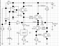
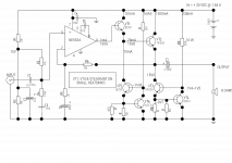
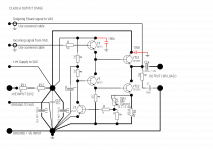
I have included a complete schematic showing the ne5534 vas and the variation of jerluwoos driver / output stage and also the power supply filter. The PS filter is only for use with the bench power supply, A separate supply would need much larger capacitors.
Gordon.
EDIT: The supply voltage after the PS filter was 23V8 not 30V as previously. ( The input to the filter was ~ 26V )
The quiescent current of both driver and output transistors were on the low side. After some investigation it was decided that the two 3k3 resistors were too high, starving the lower bd139 of base current. These were replaced with 750R resistors making the current in these resistors about 10 times the base current required by the lower bd139, the circuit worked fine at DC.
Testing with signal generator and 7.6R resistive load on output, with 'scope to view output waveform
Gain correct.
Able to reach 14v pk to pk with sinewave input, beyond this the circuit clips then "collapses" into a nasty spikey waveform. Also the current consumption fluctuates.
Stranger behavior with a square wave input. Is OK up until output exceeds about 6v pk to pk, then collapses again into spikey waveform and fluctuating supply current.
Note that with the sinewave input, the trough part of the waveform ( around the negative peak ) is blurry. Could that be parasitic oscillations?
I've heard that the ring of two CCS can be inclined to oscillate, any thoughts on rectifying this?
I have included a complete schematic showing the ne5534 vas and the variation of jerluwoos driver / output stage and also the power supply filter. The PS filter is only for use with the bench power supply, A separate supply would need much larger capacitors.
Gordon.
EDIT: The supply voltage after the PS filter was 23V8 not 30V as previously. ( The input to the filter was ~ 26V )
Attachments
Last edited:
- Status
- This old topic is closed. If you want to reopen this topic, contact a moderator using the "Report Post" button.
- Home
- Amplifiers
- Solid State
- Hot stuff- 2w Bipolar Class A Amplifier - A newbies first effort