Dear Diy'ers,
I'm feeling confident enough about the current state of this amplifier design to show it to you guys.
Please have a look into the attached document. I've tried to put all information into there including links to other threads. To encourage some interest I've attached already some pictures
This amp will be build, only it will take some time. I also have to put some time into my family offcourse (daugther of 1year old).
My previous amp kept me busy for about 1.5year.
If you guys see some opportunity's to make it better or if there are remarks, please let me know!
Attachments
Member
Joined 2009
Paid Member
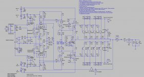
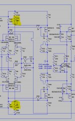
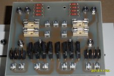
Very well engineered power supply.
It looks like the 2X59V driver regulator circuits are under the protection board.
It looks like the output voltage supply is a C-R-C topology using fuses for the R elements. An AC slow start circuit before the main transformer will remove repeated surge currents which can gradually degrade these short length fuse R elements. Long serpentine PC board traces that can distribute surge currents plus heat are often used as R's. A heatsink for the power rectifiers is often included, just to be cool.
If you "voice" your amp mainly from Spice simulation harmonic distortion data, then high hfe=500, low noise(nf=0.6db) bipolar transistors like the BC550C, BC560C, and VAS transistors like KSA1381 and KSA1186 can sim 20x-50x lower THD than MOSFET circuits using the irf610, irf9610, irf710. Most modern bipolar amps can LTSPICE sim to 0.00005% THD at 200 watts, and maintain this low THD over diverse loads through near-optimal Vbias thermal tracking circuits. A read (re-read) of Bob Cordell's book thread covers most modern bipolar circuits. Cascodes, current mirrors, tracking current sources, 3T outputs, dual slope Vbe bias, etc... Cheap to try a few LTSPICE sims before you commit to your MOSFET driver design. Bipolar+feedback philosophy= "It is better to significantly beat down THD than to worry if the TINY 3rd/odd harmonics are higher than the TINY 2nd/even harmonics."
If you "voice" your amp mainly from listening tests, then a few talented designers like Arye support your all-FET front-end preference. FET second order non-linear distortion vs. BJT odd order. I bet that Arye caliber companies perform extensive parametric testing of each MOSFET because of the wide production variation common in MOSFETS. The datasheets for irf610, irf9610, irf710 show a 2V variation in Vt, and only give a minimum gs spec. A Monte Carlo analysis quickly shows parameter variation effects.
Your 3pF Miller VAS compensation seems small, and worth a few stability sims.
A more advanced Vbe multiplier with two gain transistors as discussed by Jim Hagerman and others has shown good value. Have you run multi-temp simulations?
2SC2922 temp={t}
.step param t list 30C 80C
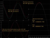
YOURS THD 20KHz 1Wrms = 0.000038%
BIPOLAR THD: 20KHz 1Wrms = 0.000002% 30C output stage
BIPOLAR THD: 20KHz 1Wrms = 0.000003% 80C output stage
YOURS THD: 20KHz 10Wrms = 0.00013%
BIPOLAR THD: 20KHz 10Wrms = 0.000007% 30C output stage
It looks like the 2X59V driver regulator circuits are under the protection board.
It looks like the output voltage supply is a C-R-C topology using fuses for the R elements. An AC slow start circuit before the main transformer will remove repeated surge currents which can gradually degrade these short length fuse R elements. Long serpentine PC board traces that can distribute surge currents plus heat are often used as R's. A heatsink for the power rectifiers is often included, just to be cool.
If you "voice" your amp mainly from Spice simulation harmonic distortion data, then high hfe=500, low noise(nf=0.6db) bipolar transistors like the BC550C, BC560C, and VAS transistors like KSA1381 and KSA1186 can sim 20x-50x lower THD than MOSFET circuits using the irf610, irf9610, irf710. Most modern bipolar amps can LTSPICE sim to 0.00005% THD at 200 watts, and maintain this low THD over diverse loads through near-optimal Vbias thermal tracking circuits. A read (re-read) of Bob Cordell's book thread covers most modern bipolar circuits. Cascodes, current mirrors, tracking current sources, 3T outputs, dual slope Vbe bias, etc... Cheap to try a few LTSPICE sims before you commit to your MOSFET driver design. Bipolar+feedback philosophy= "It is better to significantly beat down THD than to worry if the TINY 3rd/odd harmonics are higher than the TINY 2nd/even harmonics."
If you "voice" your amp mainly from listening tests, then a few talented designers like Arye support your all-FET front-end preference. FET second order non-linear distortion vs. BJT odd order. I bet that Arye caliber companies perform extensive parametric testing of each MOSFET because of the wide production variation common in MOSFETS. The datasheets for irf610, irf9610, irf710 show a 2V variation in Vt, and only give a minimum gs spec. A Monte Carlo analysis quickly shows parameter variation effects.
Your 3pF Miller VAS compensation seems small, and worth a few stability sims.
A more advanced Vbe multiplier with two gain transistors as discussed by Jim Hagerman and others has shown good value. Have you run multi-temp simulations?
2SC2922 temp={t}
.step param t list 30C 80C
YOURS THD 20KHz 1Wrms = 0.000038%
BIPOLAR THD: 20KHz 1Wrms = 0.000002% 30C output stage
BIPOLAR THD: 20KHz 1Wrms = 0.000003% 80C output stage
YOURS THD: 20KHz 10Wrms = 0.00013%
BIPOLAR THD: 20KHz 10Wrms = 0.000007% 30C output stage
Attachments
Last edited:
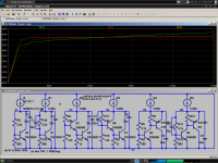

Fig2.. Vbe multipliers showing value of 2 gain transistors.
Very interesting comparison of various "zener substitute" versions.
It would be very interesting, and many I guess would be thankful, for adding the Fig2 by transient responce simulations, when CS current jumps from 5 to 15mA, for instance. And you might exclude additional caps from the circuits, just interesting how transistors do themselves.
Line Source, what sort of R can one expect from those traces?
Hi Bear,
CRC is especially effective when the amp is operating in class A
1oz copper, 0.2inch_wide * 20inch long PCB trace ~0.05 ohms
One CRC Example.
60,000uF R=0.01 60,000uF CRC
11amps into 4ohms generates 0.56V ripple
R = 0.01 ohms generates 0.56V ripple
R = 0.1 ohms reduces to 0.230V ripple
R = 0.2 ohms reduces to 0.115V ripple
R = 0.5 ohms reduces to 0.054V ripple
VOLTAGE DROP DATA:
50.94V - 50.38V 0.01ohm 0.56V ripple
49.77V - 49.55V 0.1ohm 0.23V ripple
48.625V - 48.51V 0.2ohm 0.115V ripple
45.546V - 45.492V 0.5ohm 0.054V ripple
Last edited:
Very well engineered power supply.
It looks like the 2X59V driver regulator circuits are under the protection board.
It looks like the output voltage supply is a C-R-C topology using fuses for the R elements. An AC slow start circuit before the main transformer will remove repeated surge currents which can gradually degrade these short length fuse R elements. Long serpentine PC board traces that can distribute surge currents plus heat are often used as R's. A heatsink for the power rectifiers is often included, just to be cool.
If you "voice" your amp mainly from Spice simulation harmonic distortion data, then high hfe=500, low noise(nf=0.6db) bipolar transistors like the BC550C, BC560C, and VAS transistors like KSA1381 and KSA1186 can sim 20x-50x lower THD than MOSFET circuits using the irf610, irf9610, irf710. Most modern bipolar amps can LTSPICE sim to 0.00005% THD at 200 watts, and maintain this low THD over diverse loads through near-optimal Vbias thermal tracking circuits. A read (re-read) of Bob Cordell's book thread covers most modern bipolar circuits. Cascodes, current mirrors, tracking current sources, 3T outputs, dual slope Vbe bias, etc... Cheap to try a few LTSPICE sims before you commit to your MOSFET driver design. Bipolar+feedback philosophy= "It is better to significantly beat down THD than to worry if the TINY 3rd/odd harmonics are higher than the TINY 2nd/even harmonics."
If you "voice" your amp mainly from listening tests, then a few talented designers like Arye support your all-FET front-end preference. FET second order non-linear distortion vs. BJT odd order. I bet that Arye caliber companies perform extensive parametric testing of each MOSFET because of the wide production variation common in MOSFETS. The datasheets for irf610, irf9610, irf710 show a 2V variation in Vt, and only give a minimum gs spec. A Monte Carlo analysis quickly shows parameter variation effects.
Your 3pF Miller VAS compensation seems small, and worth a few stability sims.
A more advanced Vbe multiplier with two gain transistors as discussed by Jim Hagerman and others has shown good value. Have you run multi-temp simulations?
2SC2922 temp={t}
.step param t list 30C 80C
YOURS THD 20KHz 1Wrms = 0.000038%
BIPOLAR THD: 20KHz 1Wrms = 0.000002% 30C output stage
BIPOLAR THD: 20KHz 1Wrms = 0.000003% 80C output stage
YOURS THD: 20KHz 10Wrms = 0.00013%
BIPOLAR THD: 20KHz 10Wrms = 0.000007% 30C output stage
Linesource,
Underneed the softstart board is the DC-blocker, have a look here:
http://www.diyaudio.com/forums/power-supplies/247239-high-performance-dual-mono-psu.html
The PSU board contains 4 diode bridges, 2 for the 36Vac secondaries of the 500VA R-core, 2 for the 9Vac secondaries of the 30VA R-core.
This enclosure will be connected to the amp using neutrik 8 pole Speakon connectors. Inside the amp enclosure there will be something like 20000µf added to each rail. The fuse and wires from PSU enlcosure to amp eclosure will create the "R" from the CRC.
I'm not chasing super low distortion figures. My goal is to have a nice harmonic spectrum using as less as possible feedback.
In my previous amp, Fet drivers did give much more detail to the music compared with 3 different pairs of bjt's as drivers.
The simulation tells me that I can leave the Miller caps out, I just put them into the LTspice file to make sure I do not forget room for these on the PCB whenever Miller caps are required. The VAS Fet's have a rather high input capacitance which takes the Miller cap function over.
Good tip about the temp simulation, I've not done this sofar.
Thanks for the info!
Where did you get those trafo's !!!
I want !
OS
Hi Os,
I bought the R-cores from Selectronic in Paris (France).
Transformateur R-CORE à fixation sur châssis 500VA - 2 x 36V - Transformateurs électriques
Linesource,
Indeed all the used FET's show a big variation in Vt in the datasheet. That wy I have implemented two trimmers.
A second funtion of those trimmers could be to adjust the DC-offset. However I'm not sure whether this is a good idea? The P an N VAS Fet could run on a to different bias current which influences what?... just thinking out loud.
I have to write myself a procedure how to startup the amp because of the 4 trimmer on the PCB (bias LTP, 2x Bias VAS, 1 x bias spreader).
Attachments
Attached 30C & 80C LTSPICE simulations of one a my bipolar designs showing Vbe bias circuit current changes, and well compensated output. A 2-transistor Vbe bias circuit is used for higher gain. There are several theads on 2-slope Vbe bias circuits. FANATICS use low voltage opamps for near perfect 2-slope compensation.
Add the temp assignment script to all bipolar output transistors, Vbe sensors, and any MOSFET pre-driver transistors attached to main heatsink. Include a .step control command for two(multiple) sims. Example.
2SC2922 temp={t} ----add "temp" script to heatsink devices
.step param t list 30C 80C ----add to control statemenet.
For my amps, I mount the bipolar predrivers on a separate heatsink so they stay near 30C(track same temp function as front-end devices).
I agree with Bear... it is necessary to match MOSFET transistors since their complex Vgs vs. Idd function will not match a patch resistor.
Charles Hansen, the really smart guy at Ayre, designed the MX-R amplifier with FET front end plus bipolar outputs, and no global negative feedback. You are not alone.
Attachments
Wow,
The temperature simulation opened up my eyes, this is a very nice tool!
I've made some changes on the bias spreader design.
In this amplifier I will be having the main heatsinks on which the OPS is mounted and a smaller heatinks for the VAS and driver FET's.
I noticed that a temperature variation on also the VAS stage has a tremendous effect on the OPS bias.
Thanks to OS (harmon Kardon 680) I have found a good Vbe multiplier to handle the bias currents when two heatsinks are used.
A temperature variation on the VAS/Driver section of 20°C creates in the simulation a OPS bias change of less than 0.5mA.
But, the Vbe multiplier for the OPS is still a bit undercompensated. Bias raises about 10mA for temperature increase of 30°C. The extra LED in series with the emitter of the Vbe multiplier already helped alot to, adding an extra LED creates to much undercompensation.
Attachments
Hi Os,
I bought the R-cores from Selectronic in Paris (France).
Transformateur R-CORE à fixation sur châssis 500VA - 2 x 36V - Transformateurs électriques
Ahhh , the key word "R-core" . Somewhere in between E-core and toroidial in
the stray fields /saturation categories. thanx !
OS
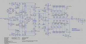
cap multiplier for front end and driver section
First of all, I made a stupid error in my last post. VAS current should not have an effect on output bias, this is offcourse one of the goals of the VBE multiplier! I just had designed a very bad one.
Now, I have been simulating some variants of cap multipliers. I would like to use a cap multiplier for the driver section and an extra RC combination for the front end. I need to drop an extra 2V for the front end to achieve nice clipping behaviour (prevent saturation of drivers and OPS).
The extra loss of voltage is not a problem for my PSU (see post 1).
A cap multiplier with a mosfet has given me the best results.
Have a look at the attachement. Is there something on which I should put more focus?
Attachments
Attached 30C & 80C LTSPICE simulations of one a my bipolar designs showing Vbe bias circuit current changes, and well compensated output. A 2-transistor Vbe bias circuit is used for higher gain. There are several theads on 2-slope Vbe bias circuits. FANATICS use low voltage opamps for near perfect 2-slope compensation.
Add the temp assignment script to all bipolar output transistors, Vbe sensors, and any MOSFET pre-driver transistors attached to main heatsink. Include a .step control command for two(multiple) sims. Example.
2SC2922 temp={t} ----add "temp" script to heatsink devices
.step param t list 30C 80C ----add to control statemenet.
For my amps, I mount the bipolar predrivers on a separate heatsink so they stay near 30C(track same temp function as front-end devices).
I agree with Bear... it is necessary to match MOSFET transistors since their complex Vgs vs. Idd function will not match a patch resistor.
Charles Hansen, the really smart guy at Ayre, designed the MX-R amplifier with FET front end plus bipolar outputs, and no global negative feedback. You are not alone.
Could you direct me to those "fanatic" near perfect dual slope compensation guys? I am probably over-thinking my first design, but the old sniff test tells me this is an under-served aspect.
re: post 4. I was just enticed to try Lateral MOSFETS as drivers for my first scratch design. Sure noise went up just a tad and yea, sim distortion up just a tad, but they are capable of sufficient output base current as you approach clipping and look in the sim to be much better behaved as far as glitches and rail sticking on clipping recovery. I have not added boosted power rails for them yet, so I am also loosing 3 dB of headroom. My amp is only 60W and I found the typical BJT's for drivers to be taxed with only two pairs of outputs.
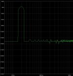
Quite enlightening to bounce around at all the points just over clipping to see how ugly things get. All kinds of things decide to glitch or oscillate even if the output looks pretty good.
Quite enlightening to bounce around at all the points just over clipping to see how ugly things get. All kinds of things decide to glitch or oscillate even if the output looks pretty good.
New ground starpoint in amp eclosure or not
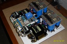
I'm having some difficulties how to do the wiring, especially the grounds.
- Inside the PSU enclosure there is one ground starpoint on top op de PCB where the PCU capacitors are on (see picture below)
- I can use two ground wires from this ground starpoint to the amp eclosure if needed (1 GND for the psu cap PCB and 1GND wire for the capmultiplier board, Front End and Driver section).
OR
Use one big ground wire to te amp enclosure and make inside the amp enclosure a new ground star point on the output side of the capacitor bank?
Attachments
- Status
- This old topic is closed. If you want to reopen this topic, contact a moderator using the "Report Post" button.
- Home
- Amplifiers
- Solid State
- 2nd amp from scratch: Low NFB- FET front end - BJT OPS