Following on after Elvee's Chop Chop Box and SGK's custom PCB implementation in post #582 of his Adventures thread, I decided to build a Transient Load Tester board too.
The idea is, to rapidly switch the load on a power supply, from high current to low current and back. A square wave of load current. This gives the power supply an opportunity to deal with a load transient, and to exhibit any instability or marginal stability in the circuitry. Since faster edge rates have higher frequency harmonics, and since power supplies might have bandwidths as high as 10 megahertz, we want steep edges and high frequency harmonics.
Building upon the experience of others, I decided to switch a low inductance load resistance right on the Transient Load Tester's PCBoard. An external resistor would provide greater flexibility, at the expense of much higher inductance due to wiring.
I also chose to optimize my Transient Load Tester board, for a single power supply output voltage: 12 volts. Again this sacrifices flexibility, but it also reduces external wiring. The load resistor is 25 ohms, implemented as six 150 ohm, 2 watt, metal film resistors in parallel. Right on the PCBoard for lowest inductance. With a 12 volt supply this gives a switched load current of 480 milliamps, which for discussion purposes below I will call "half an ampere".
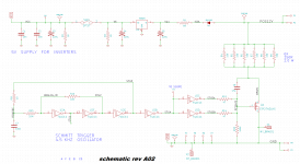
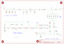
The schematic is in picture 1. Connectors P1-P4 at far right are 0.25" FastOn blade connectors, connecting the tester to (a) the PSU under test, and also optionally to (b) a fixed external resistor. This gives the option to switch between X amperes and (X + 0.5) amperes, for any X you may choose. Rexternal = 12V / (X amperes).
A low capacitance Nchannel MOSFET switches the bank of parallel load resistors in, and out, of the circuit. Since its input capacitance is relatively small (QgTOT ~ 5 nanocoulombs), I decided to use an Advanced CMOS logic chip 74HC14 as a Gate Driver, rather than a purpose built FETdriver chip capable of 1.5 amperes or 6 amperes of output current. Why switch that much current when the load is so small? It puts needlessly large current pulses in the power supply network and into the ground plane. So I used two 74HC14s in parallel (current = 24 mA each) with permanently soldered-in current limiting resistors between the driver and the load FET. In rev.A02 these resistors were 47R each; as we'll see below, that gives 80 nsec rise and fall time on the power MOSFET's gate.
I included Miller Effect capacitor C6 from gate to drain, simply as a place holder in case I feel like experimenting with it later (doubtful). Pulldown R15 discharges the MOSFET gate when switch is in the OFF position.
Since the MOSFET is a "logic level gate threshold" device, it works beautifully with low VGS. So I regulated the incoming +12V down to +5V, which means the MOSFET never sees more than 5V of VGS, comfortably less than its 20V max oxide stress spec. 5V is also the spec power supply voltage for the 74AC14 logic gate IC. Pre-load resistors R2 and R3 guarantee that the voltage regulator sees its required minimum load current, 5mA.
Isolation diode D1 makes sure that the half-ampere current squarewave is not required to drive the large onboard electrolytic capacitors C3-C5. Similarly, isolation resistor R1 ensures that C5's minuscule recharge current (when the power MOSFET cuts off and the supply voltage rises a tiny bit) does not impact the edge rate.
Three of the Schmitt Trigger inverters are used to build a 4.5 kHz oscillator. Resistors R10 and R13 add a little extra hysteresis; they widen the voltage window between Vthreshold_zero and Vthreshold_one. In retrospect this was perhaps unwise; having a low frequency analog circuit share a ground pin and bondwire inductor with a high slew rate digital circuit, simply invites trouble with ground bounce. Next time I will use 3 passive components and a dedicated CMOS 8pin oscillator IC with enormous 1/3rd supply hysteresis (7555), instead of 4 passive components and a fraction of a fast gatedriver IC. The extra cost is one 8 pin IC; the benefit is a low jitter clock with relaxed layout requirements.
The PCB layout is shown in Photo 2. Large thick grounding bars are soldered to the ground plane, to reduce DC and AC impedance between (a) MOSFET source pin and ground connector; (b) gate driver IC ground pin and MOSFET source pin. KiCad requires me to put these on the schematic, they are symbol "my_braid".
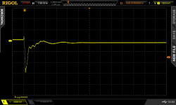
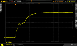
With 47 ohm current limiter resistors R12 and R14, the rising and falling waveforms on the MOSFET gate are shown in pictures 3 and 4. This is just a little slower than I would like, so I'm going to replace R12 and R14 with lower resistances and try again.
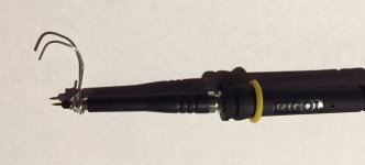
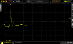
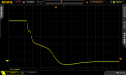
I connected the Transient Load Tester to a commercially sold power supply, the Hantek PPS2320A (link). I also connected a fixed 25 ohm resistor in parallel, so the load current switched between 0.5A and 1.0A. Waveforms are shown in pictures 5 and 6; the Hantek looks relatively well behaved with little sign of instability. To take these measurements, I fashioned a short grounding-lead for the scope probe (picture 7). The 5 inch long "ground clip" wire that shipped with the probe, distorted the waveform terribly.
_
The idea is, to rapidly switch the load on a power supply, from high current to low current and back. A square wave of load current. This gives the power supply an opportunity to deal with a load transient, and to exhibit any instability or marginal stability in the circuitry. Since faster edge rates have higher frequency harmonics, and since power supplies might have bandwidths as high as 10 megahertz, we want steep edges and high frequency harmonics.
Building upon the experience of others, I decided to switch a low inductance load resistance right on the Transient Load Tester's PCBoard. An external resistor would provide greater flexibility, at the expense of much higher inductance due to wiring.
I also chose to optimize my Transient Load Tester board, for a single power supply output voltage: 12 volts. Again this sacrifices flexibility, but it also reduces external wiring. The load resistor is 25 ohms, implemented as six 150 ohm, 2 watt, metal film resistors in parallel. Right on the PCBoard for lowest inductance. With a 12 volt supply this gives a switched load current of 480 milliamps, which for discussion purposes below I will call "half an ampere".
The schematic is in picture 1. Connectors P1-P4 at far right are 0.25" FastOn blade connectors, connecting the tester to (a) the PSU under test, and also optionally to (b) a fixed external resistor. This gives the option to switch between X amperes and (X + 0.5) amperes, for any X you may choose. Rexternal = 12V / (X amperes).
A low capacitance Nchannel MOSFET switches the bank of parallel load resistors in, and out, of the circuit. Since its input capacitance is relatively small (QgTOT ~ 5 nanocoulombs), I decided to use an Advanced CMOS logic chip 74HC14 as a Gate Driver, rather than a purpose built FETdriver chip capable of 1.5 amperes or 6 amperes of output current. Why switch that much current when the load is so small? It puts needlessly large current pulses in the power supply network and into the ground plane. So I used two 74HC14s in parallel (current = 24 mA each) with permanently soldered-in current limiting resistors between the driver and the load FET. In rev.A02 these resistors were 47R each; as we'll see below, that gives 80 nsec rise and fall time on the power MOSFET's gate.
I included Miller Effect capacitor C6 from gate to drain, simply as a place holder in case I feel like experimenting with it later (doubtful). Pulldown R15 discharges the MOSFET gate when switch is in the OFF position.
Since the MOSFET is a "logic level gate threshold" device, it works beautifully with low VGS. So I regulated the incoming +12V down to +5V, which means the MOSFET never sees more than 5V of VGS, comfortably less than its 20V max oxide stress spec. 5V is also the spec power supply voltage for the 74AC14 logic gate IC. Pre-load resistors R2 and R3 guarantee that the voltage regulator sees its required minimum load current, 5mA.
Isolation diode D1 makes sure that the half-ampere current squarewave is not required to drive the large onboard electrolytic capacitors C3-C5. Similarly, isolation resistor R1 ensures that C5's minuscule recharge current (when the power MOSFET cuts off and the supply voltage rises a tiny bit) does not impact the edge rate.
Three of the Schmitt Trigger inverters are used to build a 4.5 kHz oscillator. Resistors R10 and R13 add a little extra hysteresis; they widen the voltage window between Vthreshold_zero and Vthreshold_one. In retrospect this was perhaps unwise; having a low frequency analog circuit share a ground pin and bondwire inductor with a high slew rate digital circuit, simply invites trouble with ground bounce. Next time I will use 3 passive components and a dedicated CMOS 8pin oscillator IC with enormous 1/3rd supply hysteresis (7555), instead of 4 passive components and a fraction of a fast gatedriver IC. The extra cost is one 8 pin IC; the benefit is a low jitter clock with relaxed layout requirements.
The PCB layout is shown in Photo 2. Large thick grounding bars are soldered to the ground plane, to reduce DC and AC impedance between (a) MOSFET source pin and ground connector; (b) gate driver IC ground pin and MOSFET source pin. KiCad requires me to put these on the schematic, they are symbol "my_braid".
With 47 ohm current limiter resistors R12 and R14, the rising and falling waveforms on the MOSFET gate are shown in pictures 3 and 4. This is just a little slower than I would like, so I'm going to replace R12 and R14 with lower resistances and try again.
I connected the Transient Load Tester to a commercially sold power supply, the Hantek PPS2320A (link). I also connected a fixed 25 ohm resistor in parallel, so the load current switched between 0.5A and 1.0A. Waveforms are shown in pictures 5 and 6; the Hantek looks relatively well behaved with little sign of instability. To take these measurements, I fashioned a short grounding-lead for the scope probe (picture 7). The 5 inch long "ground clip" wire that shipped with the probe, distorted the waveform terribly.
_
Attachments
-
 TLTester_Schematic_RevA02.png43.2 KB · Views: 712
 -
 probe_ground_for_Hantek.jpg55.5 KB · Views: 249
 -
 Hantek_fall_500ma_and_500ma.png26.2 KB · Views: 185
 -
 Hantek_rise_500ma_and_500ma.png27 KB · Views: 624
 -
 MOS_gate_fall.png27.7 KB · Views: 640
 -
 MOS_gate_rise.png27.2 KB · Views: 654
 -
 theboard.JPG556.6 KB · Views: 701
Thanks Mark
Much better than my high current driver with its tenuous GND connection to the MOSFET source pin.
Or remove C6?
Was it necessary to use the 4th? (pins 3 and 4)
I decided to use an Advanced CMOS logic chip 74HC14 as a Gate Driver, rather than a purpose built FETdriver chip capable of 1.5 amperes or 6 amperes of output current. Why switch that much current when the load is so small? It puts needlessly large current pulses in the power supply network and into the ground plane.
Large thick grounding bars are soldered to the ground plane, to reduce DC and AC impedance between (a) MOSFET source pin and ground connector; (b) gate driver IC ground pin and MOSFET source pin.
Much better than my high current driver with its tenuous GND connection to the MOSFET source pin.
I included Miller Effect capacitor C6 from gate to drain, simply as a place holder in case I feel like experimenting with it later (doubtful).
With 47 ohm current limiter resistors R12 and R14, the rising and falling waveforms on the MOSFET gate are shown in pictures 3 and 4. This is just a little slower than I would like, so I'm going to replace R12 and R14 with lower resistances and try again.
Or remove C6?
Three of the Schmitt Trigger inverters are used to build a 4.5 kHz oscillator.
Was it necessary to use the 4th? (pins 3 and 4)
Last edited:
It would be interesting to see how much difference the gate drive changes will make to the Vgs waveforms. I would have thought that any added Cgd would be a negative to performance.
Given that most of the higher current load action occurs whilst the gate driver is trying to push through the Vgs turn-on region, you could always benchmark the gate driver against one of the specialist gate driver ICs by doing a custom swapout of the cmos IC in to the 14 pin header.
I wonder if that power supply can cope with battery charging?
Last edited:
The question to ask about (C6 = 47pF) connected between the MOSFET gate and the MOSFET drain, is: how does 47 pF compare to the gate-to-drain capacitance of the MOSFET itself?
Luckily CGD can be extracted from one of the figures in the MOSFET's datasheet. I'll post the figure and give readers the pleasure of analyzing it, to invent a way to extract CGD. You will know you're on the right track if you get an answer somewhere in the range (100 pF < CGD < 600 pF).
diyAudio member SGK asks whether the 4th inverter is necessary. In my opinion, it's optional but highly desirable; the 3rd inverter has got a reasonably hefty DC load (1K to AC ground --> 5mA) so why not use a "free" resource to improve the slew rate and logic levels presented to the final output drivers?
diyAudio member trobbins wonders whether the Hantek PPS2320A can be used as a battery charger? Only for smaller batteries, I expect; its max output current is only 6 amperes, as shown on the sales page linked in post#1.
_
Attachments

Last edited:
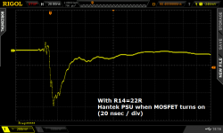
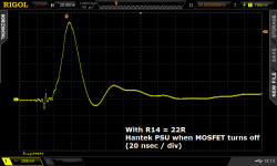
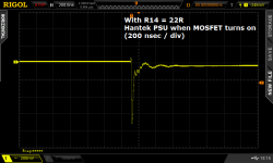
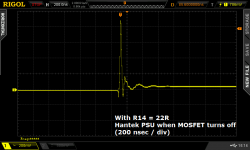
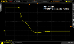
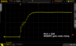
I built another of my ten (!) PCBs, this time setting the FET gate driver current-limit resistors R12 and R14 to 22 ohms. Less than half the 47 ohms used in Rev.A02 shown in post#1 above.
Results are below. MOSFET gate rise time decreased from ~80 ns to ~60 ns, and MOSFET gate fall time decreased from ~70 ns to ~55 ns. In my opinion this gives an acceptably fast turn-on and turn-off, particularly since the MOSFET drain node is such a light load (25 ohms and <10 pF) for this big macho MOSFET that's meant to switch 20 ampere loads with an on-resistance of 20 milliohms.
The Hantek power supply handled this faster switching relatively well. Although the amplitude of the deltaV pulse did increase (from 700mV to 900mV when the MOSFET turned off, and from 600mV to 730mV when the MOSFET turned on), the ringing waveshape and damping factor did not change. Stimulating the supply with steeper edges, did not reveal any new instability or marginal behavior.
_
Attachments
-
 With22R_Hantek_fall_20ns_div.png30.6 KB · Views: 108
 -
 With22R_Hantek_rise_20ns_div.png31.3 KB · Views: 102
 -
 With22R_Hantek_fall_200ns_div.png27.8 KB · Views: 100
 -
 With22R_Hantek_rise_200ns_div.png27.4 KB · Views: 106
 -
 FetGate_fall_R14_now_22R.png25.4 KB · Views: 101
 -
 FetGate_rise_R14_now_22R.png27 KB · Views: 134
Mark, was there a reason to populate C6 for the test, or was it just added at the time of fab and you felt that there was no valid reason to remove it?
Yes Cgd is very non-linear for the early stage of the transition - back when power fets started to become available, there was effectively no characterisation of those non-linearities and they were a major influence on high frequency applications (such as class E dc-dc)
Power supply transient performance was often altered by retrofitting bypass cap(s) to the supply's output terminals (either inside the supply, or at the banana plugs) - especially for vintage supplies where there were leads transferring the output from a pcb to the terminals, and only a bulk electrolytic was the last filtering cap.
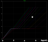
Luckily CGD can be extracted from one of the figures in the MOSFET's datasheet. I'll post the figure and give readers the pleasure of analyzing it, to invent a way to extract CGD. You will know you're on the right track if you get an answer somewhere in the range (100 pF < CGD < 600 pF).
_
I will have a go...
The first sloped portion of the graph, from origin to your red line, represents the charging of Cgs (the flatter portion to the blue line is the charging of Cgd). From eyeballing the chart with the assistance of a ruler I estimate "Qgs" to be about 1.67 nC and the voltage to be circa 3.5V at the red line. From Q = C.V I estimate Cgs to be circa 477pF.
The first sloped portion of the graph, from origin to your red line, represents the charging of Cgs (the flatter portion to the blue line is the charging of Cgd). From eyeballing the chart with the assistance of a ruler I estimate "Qgs" to be about 1.67 nC and the voltage to be circa 3.5V at the red line. From Q = C.V I estimate Cgs to be circa 477pF.
Wonderful! Congratulations for making an analysis and calculating a result! I will send you my remarks and opinions via Private Message so that I don't spoil the fun of the other diyAudio member ("trobbins") who may be working on the same problem. And countless other readers too!
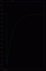
Of course the lazy man's way to "extract" CGS and CGD, is to slap together a SPICE simulation which contains a the physical test circuit that ST Microelectronics used, when they measured that Gate Charge curve attached to post#4. Then monkey around with the values of CGS and CGS for best fit to measured data.
To see how good or how awful this approach might be, I gave it a try myself; results are shown below. The Forest Green curve, marked with a white star, looks like a halfway decent match. A pleasant surprise for the lazy. I will PM the schematic of this SPICE simulation to everyone who posts here, showing their own independent analysis and calculation of the Gate-to-DRAIN capacitance, CGD. {Don't forget to compare your CGD against 47pF, which as the raison d'etre of this whole tangent}
_
Attachments
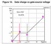
The datasheet Crss characteristic is presented as a function of Vds, and shows Crss still going up at Vds~0. Vds falls as Vgs rises, and with the low supply voltage in the example, Vdg is going to change between circa +12V and -12V.
So from the datasheet, 47pF looks fairly significant given that Cdg is shown to vary from less than 47pF to probably peak between 200 and 300pF.
So from the datasheet, 47pF looks fairly significant given that Cdg is shown to vary from less than 47pF to probably peak between 200 and 300pF.
Trobbins, don't forget that "Crss" is, by definition, an incremental small-signal model. That's what the last two letters of its name are telling you: ss = small signal. Unfortunately Crss et al are not so helpful in large signal applications like this one, where we switch the MOSFET from completely off to completely on, while swinging the device terminals many thousands of milliivolts of deltaV.
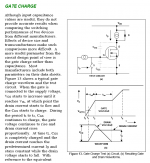
This is why power MOSFET manufacturers include Total Gate Charge specifications in their datasheets -- so that customers who apply the devices as switches, can accurately predict dwell time, rise time, gate current, and so forth. Two of the many online tutorials are excerpted below. Google Exact Phrase can find these if you wish; but they all say more or less the same thing.
_
Attachments

If I'm looking at the fine detail of waveforms during a switching transition then I get more understanding from the small signal determined level of circuit capacitances as the waveform voltages and currents dynamically change. That is equivalent to a simulation where each new calculated datapoint uses the small signal measured capacitance characteristic nowadays to get a close match to measured waveforms. I recall when spice2 power mosfet models were limited by their use of constant capacitance values, and non-linear representation of Cgd was needed in order to obtain fairly accurate waveform simulation.
Bulk charge characterisation was certainly a boon for designers to allow fast comparison between devices for applications such as switching losses in hard-switched switchmode circuits, and gate driver power consumption for lower power switchmodes .
Bulk charge characterisation was certainly a boon for designers to allow fast comparison between devices for applications such as switching losses in hard-switched switchmode circuits, and gate driver power consumption for lower power switchmodes .
To take these measurements, I fashioned a short grounding-lead for the scope probe (picture 7). The 5 inch long "ground clip" wire that shipped with the probe, distorted the waveform terribly.
Mark, I presume this was for the probe measuring Vout of the DUT rather than the probe for the trigger?
(Your package just arrived. All I can say is 'wow' and thanks! I will try to run a transient test of my 12V board ASAP.)

Here's experimental data that shows why you probably want to design your Transient Load Tester with some kind of a separate power supply for the MOSFET gate. Either a battery as in Elvee's board, or an isolation diode and a big electrolytic capacitor as used here, will do the job.
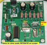
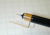
I connected up the experiment shown in Figure 1. The Transient Load Tester board was connected to a Hantek power supply through a 1 meter long cable. The cable is shown in Figure 2; it's a side-by-side "zip cord" configuration with no twisting. I attached the oscilloscope probe across nodes A and B, on the transient load tester board.
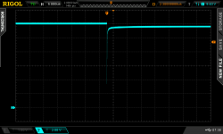
Waveforms when the MOSFET switch closes (connecting the 25R load resistor to the supply through the cable), are shown in Figures 3 and 4. You can see that the A-to-B voltage on the board, dips dramatically: from 12 volts to 3.5 volts (!). If the MOSFET switch were a standard gate-threshold device (with VTH=3.5v), it would actually cut off in this condition.
To avoid these kinds of misbehavior, we need to supply the MOSFET gate circuit with a power source that does not sag when the A-to-B voltage yanks low.
We also need a much shorter cable with much less resistance, much less self inductance (L), and as big a mutual inductance (M) as possible. Short, large-diameter, twisted wires!
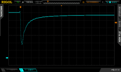
Eagle eyed readers will notice that the asymptotic voltage between A and B with the MOSFET off, is greater than the asymptotic voltage with the MOSFET on. That comes from cable resistance (big) plus power supply output impedance (small).
_
I connected up the experiment shown in Figure 1. The Transient Load Tester board was connected to a Hantek power supply through a 1 meter long cable. The cable is shown in Figure 2; it's a side-by-side "zip cord" configuration with no twisting. I attached the oscilloscope probe across nodes A and B, on the transient load tester board.
Waveforms when the MOSFET switch closes (connecting the 25R load resistor to the supply through the cable), are shown in Figures 3 and 4. You can see that the A-to-B voltage on the board, dips dramatically: from 12 volts to 3.5 volts (!). If the MOSFET switch were a standard gate-threshold device (with VTH=3.5v), it would actually cut off in this condition.
To avoid these kinds of misbehavior, we need to supply the MOSFET gate circuit with a power source that does not sag when the A-to-B voltage yanks low.
We also need a much shorter cable with much less resistance, much less self inductance (L), and as big a mutual inductance (M) as possible. Short, large-diameter, twisted wires!
Eagle eyed readers will notice that the asymptotic voltage between A and B with the MOSFET off, is greater than the asymptotic voltage with the MOSFET on. That comes from cable resistance (big) plus power supply output impedance (small).
_
Attachments


Use at 20.75v 80mA ?
I'm wondering how hard it would be to use your tester with a 20.75v 80mA regulator. The bank of 6 x 150R/2W resistors could be reduced to 2 x 510R/1W. The voltage rating of C5 may need to be increased as well.
Would any other changes be needed?
Do you sell the boards?
I'm wondering how hard it would be to use your tester with a 20.75v 80mA regulator. The bank of 6 x 150R/2W resistors could be reduced to 2 x 510R/1W. The voltage rating of C5 may need to be increased as well.
Would any other changes be needed?
Do you sell the boards?
I have 4 blank boards left; I would be happy to give you one of them for free. PM me your mailing address inside the continental USA.I'm wondering how hard it would be to use your tester with a 20.75v 80mA regulator. The bank of 6 x 150R/2W resistors could be reduced to 2 x 510R/1W. The voltage rating of C5 may need to be increased as well.
Would any other changes be needed?
Do you sell the boards?
Today is Friday; on Monday I will post the Gerber Files and the Bill Of Materials so that anyone can have a batch of boards made. I had mine made at Elecrow, but I've also had great success at Seeed and at DirtyPCBs and Shenzhen2U and Maker Studio and Smart Prototyping. All of whom I discovered through the excellent website PCB Shopper » A Price Comparison Site for PCBs . I think I paid USD 20.00 for a batch of ten PCBs.
To adapt the board for higher-than-12V operation, you will first want to choose the resistance value of the 6 parallel load resistors. I strongly suggest that if you're going to dissipate "N" watts per resistor, you select resistors whose wattage rating is at least 3*N watts. That way they'll get hot but not instant-flesh-melting hot. Read wikipedia and other sources to find out which resistor types are inductive, and then avoid those types. I chose metal film resistors because they are low inductance and the two watt versions are widely available at low cost.
The MOSFET itself is only rated for 30 volts from drain to source: (datasheet). So if you're going to connect this PCB thing to a power supply using a looooong cable, there might be a large overshoot when the MOSFET turns off and you get big L*dI/dt flyback voltage across the test terminals. Look at post #14 here in this thread; the downspike was 71% of the power supply voltage. If you get an upspike of (1.71 * 20.75 = 35.4 volts), you're exceeding the MOSFET absolute maximum rated voltage.
One solution is to remember Henny Youngman: "Doctor it hurts when I do this. Don't do that." Don't connect the Transient Load Tester board to the power supply with 1 meter long cables.
Another solution is to add a 27 volt Zener diode across the supply terminals of the Load Tester board. It won't turn on in normal operations (20.75V) but it will clamp any super high voltage flyback and protect the MOSFET. Try it in LTSPICE; build a simulation that matches the waveforms in post #14 for Vin=12V, then crank up Vin to 20.75V and look at the flyback with, and without, the zener. BTW DigiKey has 36,000 pieces of 1N5254B (27V zener) on the shelf, at $0.19 apiece.
Another solution is to use a different MOSFET. Unfortunately all the good MOSFETs are surface mounted; this one is the only decent performer in thru hole.
Finally, as you noted, the components at the input to the 5V regulator IC will need to be rated for 35V or higher. The 7805 is OK but electrolytic cap C5 needs checking. Its footprint is 10mm diameter with 5mm lead spacing.
The zener accross the chop chop box's input seems like a good idea, regardless of what SPICE may say.
I had a little go at the SPICE simulation anyway, but I'm having some difficulty believing the simulation result when the switch opens. It's discouraged me from trying to tune it to mimic the oscillographs in post #14. As you remark, zeners are quite cheap.
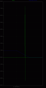
In the spice graphs the blue line is the control voltage for the switch, and the green line is the voltage at point A. Note that the blue line has rise and fall times of 1ns, which gives the best indication of the graphs' horizontal scales.
When the switch opens SPICE's voltage transient at point A is hyper fast (total duration aprox 50e-12s) with a few cycles of ringing, and max and min values that seem unrealistically large. And this is after reducing the self inductance and increasing the coupling coefficient to values that seem a bit extreme to my (rather unpracticed at these things) mind.
Am I doing something wrong? (This is the 1st time I've simulated mutual inductance.) Is the simulation no good because of missing things like stray capacitance? Is the result for real? (In which case on what scope do you experimentally verify it?) Or what?
And, finally, of course I'll do everything to absolutely minimize the length of the wires between the PSU under test and the chop chop box. I want my PSU design to look as good as poss.🙂
I had a little go at the SPICE simulation anyway, but I'm having some difficulty believing the simulation result when the switch opens. It's discouraged me from trying to tune it to mimic the oscillographs in post #14. As you remark, zeners are quite cheap.
In the spice graphs the blue line is the control voltage for the switch, and the green line is the voltage at point A. Note that the blue line has rise and fall times of 1ns, which gives the best indication of the graphs' horizontal scales.
When the switch opens SPICE's voltage transient at point A is hyper fast (total duration aprox 50e-12s) with a few cycles of ringing, and max and min values that seem unrealistically large. And this is after reducing the self inductance and increasing the coupling coefficient to values that seem a bit extreme to my (rather unpracticed at these things) mind.
Am I doing something wrong? (This is the 1st time I've simulated mutual inductance.) Is the simulation no good because of missing things like stray capacitance? Is the result for real? (In which case on what scope do you experimentally verify it?) Or what?
And, finally, of course I'll do everything to absolutely minimize the length of the wires between the PSU under test and the chop chop box. I want my PSU design to look as good as poss.🙂
Attachments

Last edited:
As promised here are the PCB manufacturing data ("Gerber files" in a .zip archive) and schematic of Rev.B. I'll be at a jobsite the rest of today and perhaps tomorrow, will catch back up here when that is completed.
Rev.B schematic and PCB are up to date; Rev.A PCB has some old, obsolete, and doesn't-work-very-well component values on the top layer text ("silkscreen"). If you're one of the unlucky few to own a Rev.A board, please stuff it according to the rev.B component values.
Rev.B schematic and PCB are up to date; Rev.A PCB has some old, obsolete, and doesn't-work-very-well component values on the top layer text ("silkscreen"). If you're one of the unlucky few to own a Rev.A board, please stuff it according to the rev.B component values.
Attachments
- Status
- Not open for further replies.
- Home
- Amplifiers
- Power Supplies
- Another PSU Transient Load Tester ("chop chop box")