Predictions of the Future
Thanks for a thought provoking post.
<<<
1. What's the largest value of Miller capacitor C6 that I will ever try, or use?
>>>
What attracted me to using this board was my guess that it's probably the square wave current load with the most insanely fast edges easily available to me. In LTSPICE my regulator responds fairly decently to a 100 ns 80 mA edge, staying within a 1/2 mv of the correct voltage (the attached plot's at 0.05 mv/div vertical & 500 ns/div horizontal). It's slightly decompensated to improve response at the lower frequencies more likely to be encountered in audio use.
I'm intending to use the very shortest possible connection between the regulator and the chop chop box.
I really really hope I don't have to slow down the chop chop box's edges, though SGK's adventures thread is certainly a lesson in the difficulty of simply getting meaningful measurements in the 1st place, and in the advantages of sloth for that purpose. The MOSFET's datasheet says 12 pF for Crss at 20 v Vgd, so 47 pF is already 4 times Crss -- the technique of swamping parameters subject to manufacturing variation in order to make their values controlled, I assume.
Sticking my finger in the air and taking a guess, I predict that in the future I won't want more than 2nF for C6. That's more than 42 times the current value!
<<<
2. What's the highest frequency at which I will ever run the square wave oscillator?
>>>
I hadn't even thought about this!
Initially I'd like to test with enough time between the rising and falling edges for everything to settle down. So that each edge's behavior's independent of the other. But now that it's drawn to my attention, when I look at the LTSPICE plot it does look like a falling edge about 500 ns after the rising edge might be a nicely awkward moment for the regulator. This suggests it could be worth pushing the frequency out to 1 MHz or more. Given the 100 ns rise and fall times, 2 MHz is probably close to the limit of what's worth trying.
So, I'm answering this question with 2MHz. I feel that this is a "more solid" answer than my guess about the maximum Miller capacitance.
In my next post I'll say what I think this all implies for the value of R1. I'd do it now, except that it's getting rather late. So for the moment there's just time for a thought about C7's contribution to the current through R1.
C7's contribution to the current through R1's independent of frequency, and can be calculated from the experimental observation that 100nF yields 4.5KHz. Viz
I = fCV
where I = average current through C7, f = frequency, C = value of C7, V = voltage C7 charges/discharges through (5 v).
And the frequency's inversely proportional to the value of C7, so
f = K/C
for some constant of proportionality K.
Substitute the latter's expression for f into the former
I = (K/C)CV
I = KV
The value of V is known, it's the 5 v that C7 charges/discharges thru, and the value of K can be computed from f = K/C and the experimental observation that 100 nF produces 4.5 kHz, viz
f = K/C
4.5E3 = K/100E-9
K = 4.5E3*100E-9 = 4.5E-4
Now substitute K = 4.5E-4 and V = 5 into I = KV
I = KV = 4.5E-4*5 = 2.25 mA
Funnily enough, that's the exact same number for C7's load current as in my previous post, it's just that this time round I've been prodded to notice that it's independent of frequency.
I think the first thing you need to do is make a couple of predictions about the future:
Thanks for a thought provoking post.
<<<
1. What's the largest value of Miller capacitor C6 that I will ever try, or use?
>>>
What attracted me to using this board was my guess that it's probably the square wave current load with the most insanely fast edges easily available to me. In LTSPICE my regulator responds fairly decently to a 100 ns 80 mA edge, staying within a 1/2 mv of the correct voltage (the attached plot's at 0.05 mv/div vertical & 500 ns/div horizontal). It's slightly decompensated to improve response at the lower frequencies more likely to be encountered in audio use.
I'm intending to use the very shortest possible connection between the regulator and the chop chop box.
I really really hope I don't have to slow down the chop chop box's edges, though SGK's adventures thread is certainly a lesson in the difficulty of simply getting meaningful measurements in the 1st place, and in the advantages of sloth for that purpose. The MOSFET's datasheet says 12 pF for Crss at 20 v Vgd, so 47 pF is already 4 times Crss -- the technique of swamping parameters subject to manufacturing variation in order to make their values controlled, I assume.
Sticking my finger in the air and taking a guess, I predict that in the future I won't want more than 2nF for C6. That's more than 42 times the current value!
<<<
2. What's the highest frequency at which I will ever run the square wave oscillator?
>>>
I hadn't even thought about this!
Initially I'd like to test with enough time between the rising and falling edges for everything to settle down. So that each edge's behavior's independent of the other. But now that it's drawn to my attention, when I look at the LTSPICE plot it does look like a falling edge about 500 ns after the rising edge might be a nicely awkward moment for the regulator. This suggests it could be worth pushing the frequency out to 1 MHz or more. Given the 100 ns rise and fall times, 2 MHz is probably close to the limit of what's worth trying.
So, I'm answering this question with 2MHz. I feel that this is a "more solid" answer than my guess about the maximum Miller capacitance.
In my next post I'll say what I think this all implies for the value of R1. I'd do it now, except that it's getting rather late. So for the moment there's just time for a thought about C7's contribution to the current through R1.
C7's contribution to the current through R1's independent of frequency, and can be calculated from the experimental observation that 100nF yields 4.5KHz. Viz
I = fCV
where I = average current through C7, f = frequency, C = value of C7, V = voltage C7 charges/discharges through (5 v).
And the frequency's inversely proportional to the value of C7, so
f = K/C
for some constant of proportionality K.
Substitute the latter's expression for f into the former
I = (K/C)CV
I = KV
The value of V is known, it's the 5 v that C7 charges/discharges thru, and the value of K can be computed from f = K/C and the experimental observation that 100 nF produces 4.5 kHz, viz
f = K/C
4.5E3 = K/100E-9
K = 4.5E3*100E-9 = 4.5E-4
Now substitute K = 4.5E-4 and V = 5 into I = KV
I = KV = 4.5E-4*5 = 2.25 mA
Funnily enough, that's the exact same number for C7's load current as in my previous post, it's just that this time round I've been prodded to notice that it's independent of frequency.
Attachments

I'm still puzzled
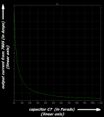
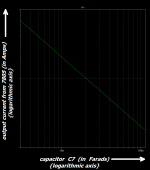
As many will know in their bones, when you see a straight line on a log log plot it implies a relation of the form of y = ax^b, where a and b are constants. The slope of the line gives the power b, and its intercept with the vertical line x = 1 gives the multiplier a. Even without vertical axis labels the slope of the line in the log log plot is discernible as -1, since moving along the line 1 decade rightwards also movers 1 decade down. So y = ax^-1 I.E. y = a/x. In this case y is I, the load current drawn from the 7805, and x is the value of C7. Thus
I = a/C7
The linear plot is consistent with this, having the familiar shape of y = 1/x. Of course, without vertical axis labels the linear plot's also consistent with y = b + a/x, since adding b just moves the curve up or down, and multiplying by a just stretches or shrinks the vertical axis. But the log log plot clearly indicates just y = a/x, with nothing added (I.E. b = 0).
C7 sets the frequency, which is inversely proportional to C7. So I = a/C7 is saying I is proportional to frequency. This makes sense for a purely capacitive load. Each capacitor charges once per cycle. Doubling the number of cycles per second doubles the number of times the capacitors must be charged and thus doubles the average current drawn.
What's puzzling though is that when I look at the REV.B circuit diagram, I see some none capacitive loads on the 7805. Notably R2 and R3, which draw a standing current of 5 mA.
Also, in my previous post I argued that the load on the 7805 from the average current through C7 is also constant with respect to frequency. Although C7 is a capacitor, and is charged once per oscillator cycle, it's also the part setting the frequency. Halve it to double f, and though it's charged twice as often, it's only half the capacitance that must be charged. Seems like a QED doesn't it: an unassailable watertight rational argument that simply cannot be wrong.
I'm guessing that the missing standing current from R2 and R3 is because they weren't in the simulation that produced the graphs.
Leaving only the question of the failure of my reasoning about C7. The algebra's not wrong, so the problem must be in my understanding of the circuit in the first place.
Prompted by that straight line on the log log plot, I can see a few places where I went wrong. All to do with how the oscillator works. One moral is don't rush to judgement, I hadn't even bothered to calculate the pole frequency for 1K and 100nF. It's 1.592 kHz, rather less than the 4.5 kHz oscillator frequency. At 4.5 kHz I calculate an attenuation of 0.333 and a phase shift of 70.5 degrees.
So C7 isn't charged and discharged through anything like the full 5 v, more like 1.67 v. And that's assuming the voltage at the output of U2E swings through the full 5 v. It might not, for the circuit to work it would only have to swing through the hysteresis voltage on U2B's input. I'd guess it's pretty much the full 5 v though, but it's a weak guess, I've really no very good idea at all. Also, because both pole frequency and oscillator frequency are inversely proportional to the same thing, C7, it still looks like C7 draws a constant current independent of frequency, unless the peak to peak voltage swing at U2E's output changes with frequency, or something else I haven't thought of.
By this point something started dawning on me. I'd been assuming that a 74AC14 output is always at either 5 v or 0 v -- like a "perfect" digital chip. But, of course, it's made from an analogue circuit on the inside. Could it be that the circuit inside the 74AC14 operates in a linear mode when it's input moves slowly (by digital standards) through it's transition voltages? Could current drawn in such a linear mode account for the current being strictly inversely proportional to C7, without any constant standing current? It seems a bit weird for this to produce a current load rising with frequency though. Obviously what happens depends on what's inside the 74AC14.
The Fairchild 74AC14 datasheet I've been looking at doesn't include an internal circuit diagram, and gives no information on any linear operating modes. I looked online for a 74AC14 spice model, but I only found a digital one, characterizing it in terms of propagation delays, etc. Without knowing more about the 74AC14 the value of further speculation is dubious.
MJ must have an LTSPICE model for the 74AC14 to produce the graphs shown.
Anyway, since I'm still puzzled, I decided to post what I've thought so far, and see if anyone else can explain the expression I = a/C7, particularly the absence of any constant standing current load on the 7805.
The voltage regulator supplies power to the first 3 logic gates (the "oscillator") and also to the final 3 logic gates (the "output driver"). C7 controls the frequency of the oscillator.
I only took a quick glance, but I don't think I see see any mention of the output driver and its load (the load is simply the capacitance it drives, i.e. the capacitance "looking into" the MOSFET gate, including Miller Effect and nonlinearities and other ick-ptui).
In the first halfcycle, the output driver sucks a packet of positive charge from its +5V supply, and places that charge on the MOSFET gate. In the second halfcycle, the output driver steers that packet of positive charge, to its GND supply.
Some number "Q" coulombs of positive charge, are pulled from the +5V supply, placed on the MOSFET gate, and then steered to GND, on every cycle. This happens "f" times per second where f is the frequency of the oscillator. In one second, Q*f coulombs are transferred from +5V to GND. I checked Wilkipedia and found out that the SI unit for Coulombs/Second is the Ampere. Conclusion: the output stage draws a current of Q*f amperes from the +5V supply. (This is a loooong term average, meaning an average over many cycles of the oscillator. In the case of an f=4500Hz oscillator, averaging over 4500 cycles (1 second) seems more than adequate).
Last edited:
PART 1
I'm sorry.
What's happened is I've been writing about the stuff I don't understand, and leaving out the stuff I do understand.
I need to be clear about what is *NOT* puzzling me, as well as about what is puzzling me.
PART 2
My question is *NOT* why is there a term in the current drawn from the 7805 inversely proportional to C7, I'M EXPECTING A TERM OF THAT FORM, and in the appendix to this post will estimate the constant of proportionality from datasheet info for the current drawn by the 74AC14, the STP27N3LH5 and C6 as 2.7E-12 A/F. BTW, the reasons for bothering with the appendix are so that anyone who spots errors in it can point them out to me, and to give people helping me a better feel for what I do and don't already understand.
MY QUESTION IS WHY ISN'T THERE AN ADDITIONAL CONSTANT CURRENT on top of the proportional to frequency current drawn by the 74AC14, the STP27N3LH5 and C6?
How do I know there isn't such an additional constant current term?
Because of the straightness of the line in the log log plot (I attach a log log plot of y = 6 + 2.7/x -- so people can see how adding the 6 makes the line not straight).
Why do I expect an additional constant current term?
Most obviously, on the REV.B circuit diagram resistors R2 and R3 draw a constant 5 mA from the 7805.
Also, if we reduce C7's value by a factor of 2 we double the frequency. Consider what happens to the average current through C7 when we reduce C7's value by a factor of 2. The amount of charge it pumps from 5 v to GND per cycle is halved, but there are twice as many cycles because the frequency's doubled. Obviously, twice as many cycles, each pumping half as much charge, results in no net change to the rate at which C7 pumps charge to GND, even though the frequency's doubled.
The same reasoning applies whether it's a factor of 2 or 3 or any other number. This is the gist of why I've been expecting the current C7 draws from the 7805 not to vary, even when frequency's changed by changing C7's value. I put this argument in algebra in my 1st post on this page.
PART 3
Here, for a moment, is some of the stuff I do understand. (Or, at least, I think I understand ... 🙂)
I had realized a while back that the entire 74AC14 (max quiescent current 20E-6 A from the datasheet, assuming no linear modes), the STP27N3LH5, and the miller capacitor C6 could be very well modeled for power dissipation purposes as a single capacitor. You can see an expression for the average current drawn by a capacitor at a frequency in use regarding C7 in the following quote from my first post on this page
Since a capacitor obeys Q = CV the expression I = fCV is equivalent to I = fQ, the expression you develop here
By reasoning shown in this post's appendix I think that at a frequency f the 74AC14, the STP27N3LH5 and C6 draw from the 7805 a total current of
I = 6E-9f [ I in amps, f in Hertz ]
APPENDIX
I estimate the total equivalent total power dissipation capacitance for the 74AC14, the STP27N3LH5 and C6 as follows
From the STP27N3LH5's datasheet (http://www.st.com/web/en/resource/technical/document/datasheet/CD00232223.pdf) Figure 10. Gate charge vs gate-source voltage, it looks like it takes near enough 5 nC to raise the STP27N3LH5's gate from 0 to 5 v. The equivalent capacitance is
C = Q/V = 5E-9/5 = 1 nF
The 74AC14's datasheet (https://www.fairchildsemi.com/datasheets/74/74AC14.pdf) quotes an equivalent power dissipation capacitance of 25 pF per gate (of which there are 6), giving a total of
6*25 = 150 pF.
And C6 contributes
47 pF
Adding it all up
1 nF + 150 pF + 47 pF = 1.197 nF, near enough 1.2 nF.
So I would expect the 74AC14, the STP27N3LH5 and C6 to draw from the 7805 a current of
I = f*Cpd*V = f*1.2E-9*5 = 6E-9*f
Since the frequency's inversely proportional to C7 we have
f = K/C7
Using the fact that 100 nF gives 4.5 kHz results in
K = f*C7 = 4.5E3*100E-9 = 4.5E-4
so
f = 4.5E-4/C7
and
I = 6E-9*f
gives
I = 6E-9*4.5E-4/C7 = 2.7E-12/C7
So the term inversely proportional to C7 I've been expecting is
I = 2.7E-12/C7
At 100 nF this evaluates to 0.027 mA. A lot less than the 5 mA drawn by R2 and R3.

I'm sorry.
What's happened is I've been writing about the stuff I don't understand, and leaving out the stuff I do understand.
I need to be clear about what is *NOT* puzzling me, as well as about what is puzzling me.
PART 2
My question is *NOT* why is there a term in the current drawn from the 7805 inversely proportional to C7, I'M EXPECTING A TERM OF THAT FORM, and in the appendix to this post will estimate the constant of proportionality from datasheet info for the current drawn by the 74AC14, the STP27N3LH5 and C6 as 2.7E-12 A/F. BTW, the reasons for bothering with the appendix are so that anyone who spots errors in it can point them out to me, and to give people helping me a better feel for what I do and don't already understand.
MY QUESTION IS WHY ISN'T THERE AN ADDITIONAL CONSTANT CURRENT on top of the proportional to frequency current drawn by the 74AC14, the STP27N3LH5 and C6?
How do I know there isn't such an additional constant current term?
Because of the straightness of the line in the log log plot (I attach a log log plot of y = 6 + 2.7/x -- so people can see how adding the 6 makes the line not straight).
Why do I expect an additional constant current term?
Most obviously, on the REV.B circuit diagram resistors R2 and R3 draw a constant 5 mA from the 7805.
Also, if we reduce C7's value by a factor of 2 we double the frequency. Consider what happens to the average current through C7 when we reduce C7's value by a factor of 2. The amount of charge it pumps from 5 v to GND per cycle is halved, but there are twice as many cycles because the frequency's doubled. Obviously, twice as many cycles, each pumping half as much charge, results in no net change to the rate at which C7 pumps charge to GND, even though the frequency's doubled.
The same reasoning applies whether it's a factor of 2 or 3 or any other number. This is the gist of why I've been expecting the current C7 draws from the 7805 not to vary, even when frequency's changed by changing C7's value. I put this argument in algebra in my 1st post on this page.
PART 3
Here, for a moment, is some of the stuff I do understand. (Or, at least, I think I understand ... 🙂)
I had realized a while back that the entire 74AC14 (max quiescent current 20E-6 A from the datasheet, assuming no linear modes), the STP27N3LH5, and the miller capacitor C6 could be very well modeled for power dissipation purposes as a single capacitor. You can see an expression for the average current drawn by a capacitor at a frequency in use regarding C7 in the following quote from my first post on this page
I = fCV
where I = average current through C7, f = frequency, C = value of C7, V = voltage C7 charges/discharges through
Since a capacitor obeys Q = CV the expression I = fCV is equivalent to I = fQ, the expression you develop here
Some number "Q" coulombs of positive charge, are pulled from the +5V supply, placed on the MOSFET gate, and then steered to GND, on every cycle. This happens "f" times per second where f is the frequency of the oscillator. In one second, Q*f coulombs are transferred from +5V to GND.
By reasoning shown in this post's appendix I think that at a frequency f the 74AC14, the STP27N3LH5 and C6 draw from the 7805 a total current of
I = 6E-9f [ I in amps, f in Hertz ]
APPENDIX
I estimate the total equivalent total power dissipation capacitance for the 74AC14, the STP27N3LH5 and C6 as follows
From the STP27N3LH5's datasheet (http://www.st.com/web/en/resource/technical/document/datasheet/CD00232223.pdf) Figure 10. Gate charge vs gate-source voltage, it looks like it takes near enough 5 nC to raise the STP27N3LH5's gate from 0 to 5 v. The equivalent capacitance is
C = Q/V = 5E-9/5 = 1 nF
The 74AC14's datasheet (https://www.fairchildsemi.com/datasheets/74/74AC14.pdf) quotes an equivalent power dissipation capacitance of 25 pF per gate (of which there are 6), giving a total of
6*25 = 150 pF.
And C6 contributes
47 pF
Adding it all up
1 nF + 150 pF + 47 pF = 1.197 nF, near enough 1.2 nF.
So I would expect the 74AC14, the STP27N3LH5 and C6 to draw from the 7805 a current of
I = f*Cpd*V = f*1.2E-9*5 = 6E-9*f
Since the frequency's inversely proportional to C7 we have
f = K/C7
Using the fact that 100 nF gives 4.5 kHz results in
K = f*C7 = 4.5E3*100E-9 = 4.5E-4
so
f = 4.5E-4/C7
and
I = 6E-9*f
gives
I = 6E-9*4.5E-4/C7 = 2.7E-12/C7
So the term inversely proportional to C7 I've been expecting is
I = 2.7E-12/C7
At 100 nF this evaluates to 0.027 mA. A lot less than the 5 mA drawn by R2 and R3.
Last edited:
P.S.
This is way way more attention than sizing R1 deserves. I'm pursuing the discussion out of a general desire to understand how the circuit works.
This is way way more attention than sizing R1 deserves. I'm pursuing the discussion out of a general desire to understand how the circuit works.
Remember that gate-to-drain capacitor C6 sees the Miller effect, since it's connected between the input and the output of an inverting amplifier. When the MOSFET is off, C6's left plate is at 0V and its right plate is at 5V. When the MOSFET is on, C6's left plate is at 5V and its right plate is at 0V. It's not a grounded capacitor; each plate swings the full supply voltage, and they swing oppositely ("Miller") rather than together ("bootstrap").
Now deltaQ = C * deltaV. But which deltaV is appropriate here? 5 volts? (5+5) volts? (5 * (1+gain)) volts? Hmm, it gives one furiously to think, as H. Poirot sometimes says.
Once that's squared away and agrees with simulation, then just plug in the highest frequency you can possibly imagine running, plus the largest value of C6 you can possibly imagine using, and crank out the max possible Q*f current. Done! Or simply install those values of C6 and C7 on your Transient Load Tester board and measure the current it draws. Either way will work.
Yikes! I have accidentally given a demonstration of why it's a terrible idea to write about a circuit without looking directly at the schematic while writing. I forgot that the FETGATE note swings between 0V and +5V while the DRAIN node swings between 0V and +12V! Many apologies for this error.
Here is the erroneous passage, with corrections shown in underlined bold text
Sorry for the careless mistake, I will try to do better!
Here is the erroneous passage, with corrections shown in underlined bold text
When the MOSFET is off, C6's left plate is at 0V and its right plate is at 12V. When the MOSFET is on, C6's left plate is at 5V and its right plate is at 0V. It's not a grounded capacitor; each plate swings many volts, and they swing oppositely ("Miller") rather than together ("bootstrap").
Now deltaQ = C * deltaV. But which deltaV is appropriate here? 5 volts? (5+12) volts? (((5+12/2) * (1+gain)) volts? Hmm, it gives one furiously to think, as H. Poirot sometimes says.
Now deltaQ = C * deltaV. But which deltaV is appropriate here? 5 volts? (5+12) volts? (((5+12/2) * (1+gain)) volts? Hmm, it gives one furiously to think, as H. Poirot sometimes says.
Sorry for the careless mistake, I will try to do better!
Honi soit qui mal y pense!Many apologies for this error.
You've helped me lots, and others here as well. No worries from me for an error which is trivial in its impact on the main knowledge being conveyed.
I hope the Silicon Valley tradition of learning by making mistakes not being evil also applies to diyaudio. Since I make plenty of mistake* myself, and wish to be here without shame. 🙂
* including the occasional intentional mistake.
Because my PSU under test outputs 20.75 v, I reverse the digits of the 12s to make 21s (21's near enough 20.75).
Add up the charge pumped from the 5 v supply to ground each cycle:
For the 74AC14
6 * 25 pF * 5 v = 0.75 nC
For the STP27N3LH5
5 nC
For C6
(5v + 21v) * C6 = 26 * C6
Adding it all up
5E-9 + 7.5E-10 + 26 * C6 = 5.75E-9 + 26 * C6
Multiply by f to get average current I
I = (5.75E-9 + 26 * C6) * f
Since the frequency f is inversely proportional to C7 we have
f = K / C7
Using the fact that 100 nF gives 4.5 kHz results in
K = f*C7 = 4.5E3 * 100E-9 = 4.5E-4
so
f = 4.5E-4 / C7
Substitute f = 4.5E-4 / C7 into I = (5.75E-9 + 26 * C6) * f
I = (5.75E-9 + 26 * C6) * (4.5E-4 / C7) = 4.5E-4 * (5.75E-9 + 26 * C6) / C7
So I would expect the average current I drawn from the 7805 by the 74AC14, the STP27N3LH5 and C6 to be given by
I = 4.5E-4 * (5.75E-9 + 26 * C6) / C7
Setting C6 at 47 pF gives
I = 3.14E-12 / C7
Once pointed out my mistake seems obvious. The correct deltaV for C6 is (5 + 21) volts, not 5 v as I had it in my previous estimate of the current drawn by the output stage. I correct this estimates as follows:But which deltaV is appropriate here? 5 volts? (5+21) volts? (((5+21/2) * (1+gain)) volts? Hmm, it gives one furiously to think, as H. Poirot sometimes says.
Add up the charge pumped from the 5 v supply to ground each cycle:
For the 74AC14
6 * 25 pF * 5 v = 0.75 nC
For the STP27N3LH5
5 nC
For C6
(5v + 21v) * C6 = 26 * C6
Adding it all up
5E-9 + 7.5E-10 + 26 * C6 = 5.75E-9 + 26 * C6
Multiply by f to get average current I
I = (5.75E-9 + 26 * C6) * f
Since the frequency f is inversely proportional to C7 we have
f = K / C7
Using the fact that 100 nF gives 4.5 kHz results in
K = f*C7 = 4.5E3 * 100E-9 = 4.5E-4
so
f = 4.5E-4 / C7
Substitute f = 4.5E-4 / C7 into I = (5.75E-9 + 26 * C6) * f
I = (5.75E-9 + 26 * C6) * (4.5E-4 / C7) = 4.5E-4 * (5.75E-9 + 26 * C6) / C7
So I would expect the average current I drawn from the 7805 by the 74AC14, the STP27N3LH5 and C6 to be given by
I = 4.5E-4 * (5.75E-9 + 26 * C6) / C7
Setting C6 at 47 pF gives
I = 3.14E-12 / C7
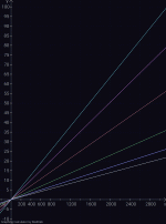
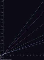
To get a better handle on how the current needed varies with frequency and value of Miller capacitor C6 I made some graphs based on the expression
I = (5.75E-9 + 26 * C6) * f
from my previous post.
The frequency's on the horizontal axis in kHz, and the current drawn by the 74AC14, the STP27N3LH5 and C6 is on the vertical axis in mA. Each line shows how current increases with frequency for a given value of Miller capacitor C6. The following values of C6 are graphed
47 pF, 100 pF, 220 pF, 470 pF, 750 pF, 1000 pF.
Looking at these graphs I can see why MJ included the option to power the chop chop board from somewhere other than the PSU under test via the 7805. At 1 MHz the current is 32 mA for a C6 of 1 nF and 7 mA for a C6 of 47 pF. At 4.5 kHz the currents are all negligible -- very comfortably under 0.2 mA.
I see 2 basic useful frequency ranges for the chop chop box. A low frequency range, where the PSU has ample time to settle after each edge, allowing the edges to be observed as separate events that don't effect 1 and other. And a high frequency range where the next edge occurs before the PSU has settled down from the previous edge.
For my shunt regulator 4.5 kHz is good for a low chop chop box frequency, and frequencies around 1 MHz might be interesting for getting the edges to interact. My sense is that for the high frequency testing I'm better off powering the chop chop box from my bench power supply rather than from it's own 7805 based supply. Even with C6 at only 47 pF the current is 7 mA at 1 MHz, almost 10% of my PSU's rated output! But at the low frequencies the 7805 should be just fine.
Attachments
Chop chop board comes to life
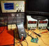
The time has come to build the chop chop board. It's embarrassing because now you can all see my decidedly below average soldering abilities. But hey, outside of Lake Woebegone, somebody has to be below average. And the board powered up and worked correctly 1st time.
You might think that having built a PSU testing board, and having 2 bench PSUs available to test, the 1st thing I'd do with it would be to test a PSU. After all, it would be good practice for testing my own regulator design, which is the main reason I became interested in this borad. But this is DIY, not work, and we are free to pursue our curiosities in whatever directions may happen to take our fancy. As anyone who's read through this thread so far will know, I've been trying to develop an expression for how the current it will draw depends on C6 and C7, before actually building the board.
So I goofed off. Instead of testing a PSU I measured the current used by the tester. I'd never let myself goof off like that on a commercial project.
I left out the 7805 and 1 of the ground pins, to make space to solder 2 wires onto the board, through which I power it from a bench PSU. My shunt regulator is a low current design, and powering the chop chop box from it would use up at least 10% of it's capacity -- more at higher frequencies and values of Miller capacitor. Offloading the task of powering the chop chop board from the PSU under test, means that the tester can always test the full capacity of the unit under test. It also makes it easy to insert a current meter into the supply for the chop chop board.
There hasn't been time to do very much yet, but I did make a few measurements because I wanted to know the current with the power MOSFET and the Miller capacitor *NOT* fitted. Later, by subtracting these numbers, it will be possible to isolate just the current used by the MOSFET and the Miller capacitor.
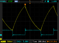
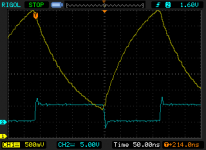
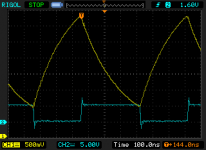
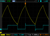
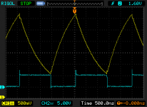
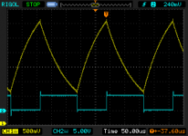
For each of these 6 measurements I attach an oscillograph showing the voltage at the trigger connection of the chop chop board (blue trace 5v square wave) and the voltage at the top of C7 I.E. point RCNODE on the circuit diagram (yellow trace, and my 1st use of a groundspring)..The photos actually show a slightly later test setup, with the MOSFET and Miller capacitor fitted, but otherwise identical.
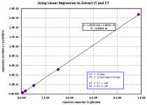
This website
Linear Regression Calculator
graphed the current (vertical axis in mA) against the frequency (horizontal axis in kHz) and did a least squares fit for a straight line, yielding the expression
I = 8.5442108428714 + 0.0013271419445407*f [ I in mA, f in kHz ]
with a correlation coefficient (r) of 0.99850660936517.
Reducing to 3 significant figures and normalizing to amps and hertz yields
I = 8.54E-3 + 1.33E-9*f
I am still thinking ...
The time has come to build the chop chop board. It's embarrassing because now you can all see my decidedly below average soldering abilities. But hey, outside of Lake Woebegone, somebody has to be below average. And the board powered up and worked correctly 1st time.
You might think that having built a PSU testing board, and having 2 bench PSUs available to test, the 1st thing I'd do with it would be to test a PSU. After all, it would be good practice for testing my own regulator design, which is the main reason I became interested in this borad. But this is DIY, not work, and we are free to pursue our curiosities in whatever directions may happen to take our fancy. As anyone who's read through this thread so far will know, I've been trying to develop an expression for how the current it will draw depends on C6 and C7, before actually building the board.
So I goofed off. Instead of testing a PSU I measured the current used by the tester. I'd never let myself goof off like that on a commercial project.
I left out the 7805 and 1 of the ground pins, to make space to solder 2 wires onto the board, through which I power it from a bench PSU. My shunt regulator is a low current design, and powering the chop chop box from it would use up at least 10% of it's capacity -- more at higher frequencies and values of Miller capacitor. Offloading the task of powering the chop chop board from the PSU under test, means that the tester can always test the full capacity of the unit under test. It also makes it easy to insert a current meter into the supply for the chop chop board.
There hasn't been time to do very much yet, but I did make a few measurements because I wanted to know the current with the power MOSFET and the Miller capacitor *NOT* fitted. Later, by subtracting these numbers, it will be possible to isolate just the current used by the MOSFET and the Miller capacitor.
Code:
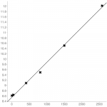
=====   ========   =====   ==========
C7/nF   Freq/kHz   I/mA    C7 pk-pk/v
=====   ========   =====   ==========
0.1     2577       12.02   3.12
0.22    1502       10.51   2.9
0.47    811.7      9.49    2.74
1       406.5      9.09    2.66
10      44.25      8.64    2.6
100     4.425      8.61    2.62
===== ======== ===== ==========This website
Linear Regression Calculator
graphed the current (vertical axis in mA) against the frequency (horizontal axis in kHz) and did a least squares fit for a straight line, yielding the expression
I = 8.5442108428714 + 0.0013271419445407*f [ I in mA, f in kHz ]
with a correlation coefficient (r) of 0.99850660936517.
Reducing to 3 significant figures and normalizing to amps and hertz yields
I = 8.54E-3 + 1.33E-9*f
I am still thinking ...
Attachments

MS Excel will perform linear regressions too. They are called "trendline" and you really want to (1) make the equation visible on the chart; and also (2) tell MSExcel that the equation display box should present the coefficients in scientific notation with 6 decimal digits after the decimal point. But at least it's on your computer and at least you can plot the measured data versus the fitted equation.
It took 12 hours for me to remember that I put an example of an Excel linear regression, in the Quasimodo design note. It's Figure 17 on page 20.
Excel's fitted trendline equation is displayed (black box) in scientific notation with four digits after the decimal, and I told it to display the goodness-of-fit statistic Rsquared too. This box comes straight from Excel and all I did was fiddle with the formatting.
The blue box lower down, is merely a "Text Box" which I created. Excel had nothing to do with this except allowing me to write it, and to place it where I wanted it on the figure. I deliberately changed the font to something very non-Excel, to indicate: hey this is just a human comment.
You can compare the numbers in the lower box versus those in the upper, to learn whether my Casio calculator made an error going from y=mx+b to LT and CT.
_
Attachments
I keep wondering how one might tweak a board such as the circuit in post 1 to transient test a negative supply... I guess one could cut the supply to D1 (from what would ordinarily be the +12V input) and power the inverters/pass transistor gate from a 9V battery.
I'm new to thinking with -ve voltages. Am I right that the same n-channel MOSFET can be used if the foregoing is done? Presumably -12Vin would be connected to the GND connector tab on the board and Supply GND to the +12V connector in order to maintain the same direction of current flow through the pass transistor. R15 should still drain the FET gate capacitance in the normal way.
I'm not sure how C6 is affected though.
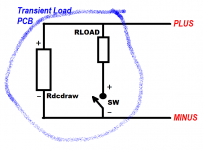
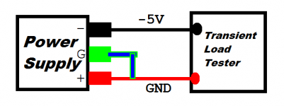
Perhaps the figure below might be helpful.
The Transient Load Test Board is represented by a very low inductance load resistor RLOAD, an ideal switch SW, and some other ancillary support circuitry that I have lumped together into a single element called Rdcdraw.
Like every single Special Relativity homework problem in University Physics 201 that you ever worked, we start here by assigning an observer and an observer's frame of reference. In this case the observer is a small creature who sits on the Transient Load Tester PCB. He looks out and sees that his two connections to the external world (named "PLUS" and "MINUS") are attached to a power supply. {maybe an oscilloscope too}
From the point of view of the observer, does it make any difference whether the outside world exclaims "GROUND IS MINUS!!" or "Ground is PLUS!" ??
If not then the selfsame PCB can test "negative 5V power supplies" and also "positive 5V power supplies", if you make certain not to connect the two leads PLUS and MINUS backwards.
Or, perhaps am I guilty of making an incorrect / incomplete / misleading diagram ? If so, please state what should have been drawn instead.
_
Attachments
Last edited:
From the point of view of the observer, does it make any difference whether the outside world exclaims "GROUND IS MINUS!!" or "Ground is PLUS!" ??
If not then the selfsame PCB can test "negative 5V power supplies" and also "positive 5V power supplies", if you make certain not to connect the two leads PLUS and MINUS backwards.
Is this not circular?
Certain circuit components which may be lumped together in your diagramme may be sensitive to what's connected to PLUS and MINUS. For example, I understand the 7805 won't regulate a negative voltage supply. Also, the 74AC14 requires a Vcc of -0.5V to 7.0V.
Where I get confused is if I try to step back and think not in absolute terms but in relative terms and conclude "GND is just a relative concept and with a negative 12V supply GND is just 12V positive with respect to -12V and hence I can connect Supply GND to the board's +12Vin tab and Supply -12V to the GND tab so that the board's 'Vin' is maintained 12V positive with respect to its 'GND' as before."
But does the 7805 regulate and the 74AC14 work? Does the FET gate charge and discharge?
Hence I found it easier to think about breaking the circuit at D1 and keeping all that drives the FET gate driven by +X volts.
But does the 7805 regulate and the 74AC14 work? Does the FET gate charge and discharge?
After further investigation I think they do. The FET charging was easier to get my head around as it is Vgs that matters and so Vg just needs to rise far enough above Vs which will be -12V. Investigating the 7805 was complicated by various internet articles saying a 7905 had to be used for a negative voltage rail but here Vin to the 7805 would actually be Supply GND and GND for the 7805 would be Supply -12V. I struggled more with the 74AC14 but I guess Vcc is, again, relative to "GND" and so again, Vcc just needs to be 2-6V above -12V.
So I would relabel Mark's graphic slightly to assist my slow brain and name the connections High and Low. So long as the board's High connection is connected to the higher supply voltage potential (GND in the case of a negative regulator) then all is fine.
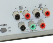
I am very happy with my PPS2320 power supply. Attachment 1 shows its front panel connectors. I will discuss the bottom set of connectors, "channel 3".
Thanks to its multi-secondary power transformer, this is a Fully Floating power supply. If you set it to "3.6 volts" then the red terminal will be 3.6 volts more positive than the black terminal. Neither red nor black are connected to ground (or "earth", or "common") -- they are Fully Floating. The user (that's me) gets to make that connection however he wishes. If I ground the black terminal, then red is +3.6V and black is GND. If I ground the red terminal, then red is GND and black is -3.6V. Cute! It's either a positive power supply or a negative power supply, depending on how I hook it up.
They also provide a green connector on the front panel, which is connected to Chassis Ground (the third wire in the AC mains cable), in case you might wish to use it. If you do then of course it is no longer Fully Floating, but is instead referenced to Chassis Ground.
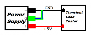
Attachment 2 shows how I connect this power supply to provide +5V and GND. Attachment 3 shows how I connect this power supply to provide GND and -5V.
Everything works just dandy in these connection; fuses don't blow, components don't overheat, connectors don't melt, and the safety GFCI (called "RCD" in UK and Ozzie) doesn't activate. But is this a lucky accident? Is it truly dangerous, and will soon explode in a bomb burst of molten copper (some of it piercing my eyeballs and genitals) at any second?
Thanks to its multi-secondary power transformer, this is a Fully Floating power supply. If you set it to "3.6 volts" then the red terminal will be 3.6 volts more positive than the black terminal. Neither red nor black are connected to ground (or "earth", or "common") -- they are Fully Floating. The user (that's me) gets to make that connection however he wishes. If I ground the black terminal, then red is +3.6V and black is GND. If I ground the red terminal, then red is GND and black is -3.6V. Cute! It's either a positive power supply or a negative power supply, depending on how I hook it up.
They also provide a green connector on the front panel, which is connected to Chassis Ground (the third wire in the AC mains cable), in case you might wish to use it. If you do then of course it is no longer Fully Floating, but is instead referenced to Chassis Ground.
Attachment 2 shows how I connect this power supply to provide +5V and GND. Attachment 3 shows how I connect this power supply to provide GND and -5V.
Everything works just dandy in these connection; fuses don't blow, components don't overheat, connectors don't melt, and the safety GFCI (called "RCD" in UK and Ozzie) doesn't activate. But is this a lucky accident? Is it truly dangerous, and will soon explode in a bomb burst of molten copper (some of it piercing my eyeballs and genitals) at any second?
Attachments
As I was thinking about the above I found Fig 11 here helpful. It also answered a question/concern I had regarding the IPP037N06L3G-based regulator circuit you helped me construct (and which led to this PSU transient load tester). There's no need for a "negative voltage regulator" version if one has dual transformer secondaries. I think I will end my investigation into boosting the current capability of the LM317+Jung/Didden SR and just use the Fig 11 configuration with the circuit I have already spent so much time on.
- Status
- Not open for further replies.
- Home
- Amplifiers
- Power Supplies
- Another PSU Transient Load Tester ("chop chop box")