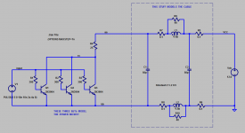
Here's a quick slapdash simulation model of the crappy 1 meter zipcord cables shown in post#14. I can't justify any of the values except to say they don't look completely crazy to me, and the resulting simulation waveforms have the same general shape as the scope photo. Don't bet your life or your money on its predictive accuracy!
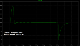
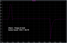
When the supply voltage cranks up to 20.75 volts, the cable-induced overshoot goes above 30V, too high for this MOSFET. So I would suggest taking active measures to prevent big overshoots from happening.
When the supply voltage cranks up to 20.75 volts, the cable-induced overshoot goes above 30V, too high for this MOSFET. So I would suggest taking active measures to prevent big overshoots from happening.
Attachments
What does the step response of an unregulated power supply look like. Iron transformer, rectifier, big output capacitor.
I doubt that anyone else is interested enough to try the experiment, or to dig out their scope photos from 8 years ago when they made a few tests and recorded the results. So I doubt you'll get an answer unless you try the experiment yourself.
Perhaps it might also be worth considering, whether this is a situation where you would believe and trust the results of a SPICE circuit simulation, or not. Maybe you don't even need to set foot in the hardware lab, to get the answers you seek.
Perhaps it might also be worth considering, whether this is a situation where you would believe and trust the results of a SPICE circuit simulation, or not. Maybe you don't even need to set foot in the hardware lab, to get the answers you seek.
Thanks to Mark Johnson
A thank-you to Mark Johnson who's package arrived today. In the next few days I'll do a Mouser order for the other parts it needs.
I have 4 blank boards left; I would be happy to give you one of them for free. PM me your mailing address inside the continental USA.
A thank-you to Mark Johnson who's package arrived today. In the next few days I'll do a Mouser order for the other parts it needs.
Attachments
I've been looking at the board, and I have a question.
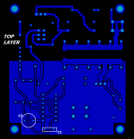
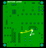
I notice 2 ground planes (1 on each side) connected in multiple places. The ground plane on the bottom covers the entire board. But the top ground plane covers only a bit more than half the board. It doesn't cover the area around the regulator positive input, the load resistors, and the 7805 & associated components. It seems like the parts uncovered by the top ground plane are all parts that might be effected by noise on the output of the power supply under test.
My question is: Why this partial coverage with the top ground plane, but not the bottom ground plane?
BOM
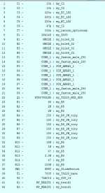
I made a minimal BOM for schematic Rev.B for normal 12v 500mA operation:
And a list of the differences for my target of 20.75v 80mA operation:
I made a minimal BOM for schematic Rev.B for normal 12v 500mA operation:
Code:
===========   ===   =============================
Designator    Qty   Item
===========   ===   =============================
R1            1 x   68R
R2,R3         2 x   2K
R4 - R9       6 x   150R 2W
R10           1 x   18K
R11           1 x   1K
R12,R14       1 x   47R
R13           1 x   3K

C1,C2         2 x   10nF
C3,C4         2 x   220uF Electrolytic 6.3v
C5            1 x   220uF Electrolytic 16v
C6            1 x   47pF
C7            1 x   100nF

U1            1 x   7805
U2            1 x   74AC14
Q1            1 x   STP27N3LH5
D1            1 x   1N4148

SW1           1 x   SPST Switch
X1,X1         2 x   Copper Braid (1/4" x 1/2")
P1,P2,P8,P9   4 x   Blade Connector
P3 - P7       5 x   Single Pin Connector
              1 x   6 pin SIL (for C7 freq. adj.)
===========   ===   =============================
Code:
===========   ===   =============================
Designator    Qty   Item
===========   ===   =============================
R4,R5         2 x   Not Fitted
R6 - R9       4 x   1K 1W
C5            1 x   220uF Electrolytic 35v
ZD1           1 x   Zener Diode 27v 1W
=========== === =============================A favorite detective novel of mine includes a scene where the detective agrees to work on a vexing problem for a group of eight lawyers, all of them Harvard graduates. The detective presents his specification of work and schedule of payments (which are punishingly high) in the form of an employment contract. This drives the lawyers insane because they are not accustomed to getting screwed by a legal contract. Finally in desperation they agree to the enormous fees and all other demeaning aspects of the contract but they insist that the detective remove the provision that they shall be be liable for the full amount "jointly and severally".Why this partial coverage with the top ground plane, but not the bottom ground plane?
Our detective protagonist blandly replies, "Of course. I only put that in so that you gentlemen would have something to take out."
Similarly on this PCB, I put in a huge visual distraction (partial plane) so that viewers would have something to complain about.
In my opinion this board works just fine as-is, and I am using it for its intended purposes myself, with great success. However if anyone wants to design a new PCB layout that has a full ground plane on the top layer, I offer my best wishes and my prediction that you will probably succeed in the endeavor. I would add a gentle reminder that if you wish, you can pay an extra $1.60 per board and have both layers made with 70 micron thick copper instead of the standard 35 microns. You can cut all resistances in half merely by writing a slightly larger check. In my opinion the boards work fine with 35mm copper, but readers should be aware they have options. "If some is good then more is better" is a commonly heard recommendation here on DIYA. In this case the price of "more" appears small.
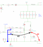
The main goal of this PCB layout is to minimize the voltages V1 and V2 shown on the attached schematic. I wanted very low resistance and very low inductance in these two layout paths. These are indicated on the Gerber plot images below. In my opinion, V1 and V2 are indeed minimized.
The plots also show the power supply bypass capacitors for the CMOS hex inverter IC -- named C1 and C3. The inverter has VCC on pin#14 (lower left of the DIP) and GND on pin#7 (upper right of the DIP). You can see that the traces from C1+C3 to ICpin14 are very short, and the traces from C1+C3 to ICpin7 are as short as possible since they are on the groundplane.
Me, I'm satisfied with it. Anyone who isn't, has my permission and blessing to make whatever improvements they wish.
_
Attachments
Maybe this will help. It's the KiCad list of footprints. The names are meaningful to me but perhaps not to anyone else, so here is an explanationI made a minimal BOM for schematic Rev.B for normal 12v 500mA operation:
- C2 . . . . . . . . . . capacitor with 0.2 inch (5 mm) lead spacing
- EC_LS2 . . . . . . . 10 mm diameter electrolytic capacitor with 0.2 inch (5 mm) lead spacing
- narrow_optioncap Socket for capacitor having 6 pins at 0.1 inch spacing
- PIN_ARRAY_1 . . . A pin to attach a scope probe or crocodile clip
- R5 . . . . . . . . . . . thru hole resistor whose drill holes are spaced 0.5 inches (12.5 mm) apart
- R6_2W_tiny . . . . . the smallest 2 watt metal film resistor DigiKey sells (0.6" lead spacing)
Attachments
Last edited:
Oh. Yes, I'd missed that. We can use the extra headroom from the higher PSU voltage to bring down the corner frequency of the 7805's input filter without added cost or complexity.Change R1 to 120R?
LOL. I like your style.I put in a huge visual distraction (partial plane)
Could you give us some information on the C6 Miller Effect capacitor. I spent a couple of hours searching for an explanation and how to calculate it, but i only found site after site talking about Miller capacitance and amplifiers. I could not find anything on switches.
SGK good link, and a surprise. The C6 miller capacitor actually slows down the switching. I thought it was put in there to speed up the switching. That for a load bank you wanted a fast straight pulse.
My next guess is that the slowdown lessens the inductive effect of the wires connecting the load bank to the power supply.
My next guess is that the slowdown lessens the inductive effect of the wires connecting the load bank to the power supply.
The PCB layout includes C6 between MOSFET gate and drain, because I wanted to have the option to play with different capacitance values there. Zero pF of extra capacitance is of course one option: merely omit C6 entirely.
But I got lucky; the physical PCB matched the SPICE simulations pretty closely, and the match got even better when I reduced the series resistors R12+R14 from 47R to 22R. So I haven't felt the need to perform further fine-tuning by adjusting the value of C6. 47pF gives what I want.
Curious readers can explore these kinds of ideas by experimenting, either with a physical board, or with an LTSPICE simulation. You can model a 74AC14 logic gate as an ideal voltage source, whose output series resistance is ~20 ohms. You can model the goofy MOSFET from ST Microelectronics, by one of the LTSPICE presupplied MOSFETS whose GateCharge is <= 5 nanocoulombs, and whose Ron is low. Luckily LTSPICE lets you click on column headers in the "Pick a MOSFET" dialog box, and sort by parameter value. You might decide that Si7218DN or IPP147N03L or BUK9K5260E could serve as possible "models" of the STP27N3LH5 . Maybe you actually want to simulate with all three, just to give yourself extra peace of mind, that you're not totally dependent on weird accidental quirks of one oddball MOSFET.
Mark said.
"I reduced the series resistors R12+R14 from 47R to 22R"
Mark since you have patents on chip design i think you can answer this question with certainty.
I always wondered about over driving the output of chips.
The 74AC14 has a DC source or sink of 50mA. You are driving the gate with 22 ohms, 5V / 22 ohms = 227mA.
Does this damage the chip and can you count on the drive current you are getting now to be consistent, if you ran a batch of these and or the chip came from different manufactures..
It may help to remember that we deliberately chose the world's best thru-hole MOSFET with the world's lowest (RdsON * Qgate) figure of merit. So this little baby has got the lowest available input capacitance, while providing the low Ron that we demand.
The capacitance itself is wildly nonlinear but we are brave people and for the purposes of estimating power and heat, we will use a simple linear approximation: CMOSFET =~approx~= GateCharge / SupplyVoltage. Thus CMOSFET =~approx~= 5E-9 / 5. Thus CMOSFET is approximately 1000 picofarads for the purposes of estimating power and heat.
Do integrated circuit I/O pins burn out when you ask them to drive 1000pF load capacitances? No they do not. Especially when you don't switch the big capacitances very often, as in this little transient load tester board: only 9000 times per second. For comparison purposes, fast digital circuits switch their I/O pins hundreds of millions of times per second (with ~ 50 pF load capacitances).
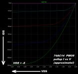
I've attached the I-V curve of an IC transistor, similar to the transistor used in the 74AC14 gate. It's a Pchannel MOSFET, used to pull up the I/O pin of a chip similar to the 74AC14. As you can see, the max current this transistor is able to pump out, is 160 mA. And it only does that if you short the output to ground so that VDS=-5.0 volts. When the output pin has risen up to within 0.5 volts of the supply (where VDS = -0.5 volts), transistor current is "only" 40 mA.
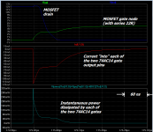
When I connect this transistor to a 22 ohm series resistor and then to the gate of our power MOSFET, I get the time domain waveforms shown in the second figure.
The green waveform is the MOSFET gate; it has that little Miller Effect Pedestal that we see in scope photos of real circuits on real PCBoards. The blue waveform is the MOSFET drain, which falls from the external power supply voltage (12V) to ground. I plotted current in red, and power dissipation (voltage * current) in blue. Neither the current nor the power, jump to ridiculously large "instant burnout" values.
Now we are able to give the final answer: No, this MOSFET's gate capacitance is so small, that two 74AC14 logic gates working in parallel can drive it easily. There's no danger of overcurrent or overheating.
The capacitance itself is wildly nonlinear but we are brave people and for the purposes of estimating power and heat, we will use a simple linear approximation: CMOSFET =~approx~= GateCharge / SupplyVoltage. Thus CMOSFET =~approx~= 5E-9 / 5. Thus CMOSFET is approximately 1000 picofarads for the purposes of estimating power and heat.
Do integrated circuit I/O pins burn out when you ask them to drive 1000pF load capacitances? No they do not. Especially when you don't switch the big capacitances very often, as in this little transient load tester board: only 9000 times per second. For comparison purposes, fast digital circuits switch their I/O pins hundreds of millions of times per second (with ~ 50 pF load capacitances).
I've attached the I-V curve of an IC transistor, similar to the transistor used in the 74AC14 gate. It's a Pchannel MOSFET, used to pull up the I/O pin of a chip similar to the 74AC14. As you can see, the max current this transistor is able to pump out, is 160 mA. And it only does that if you short the output to ground so that VDS=-5.0 volts. When the output pin has risen up to within 0.5 volts of the supply (where VDS = -0.5 volts), transistor current is "only" 40 mA.
When I connect this transistor to a 22 ohm series resistor and then to the gate of our power MOSFET, I get the time domain waveforms shown in the second figure.
The green waveform is the MOSFET gate; it has that little Miller Effect Pedestal that we see in scope photos of real circuits on real PCBoards. The blue waveform is the MOSFET drain, which falls from the external power supply voltage (12V) to ground. I plotted current in red, and power dissipation (voltage * current) in blue. Neither the current nor the power, jump to ridiculously large "instant burnout" values.
Now we are able to give the final answer: No, this MOSFET's gate capacitance is so small, that two 74AC14 logic gates working in parallel can drive it easily. There's no danger of overcurrent or overheating.
Attachments
Choosing R1
Increasing R1's resistance is advantageous because it lowers the pole frequency of the 7805's input filter without added cost or complexity. It's made possible in my case because the higher output voltage of the regulator under test (20.75 v instead of 12 v) leaves more headroom for the voltage drop across R1.
I estimate the current through R1 as being 7.3 mA plus whatever flows out of the 7805's ground pin. The 7.3 mA is 5mA through R2 & R3 plus 2.25 mA to charge 100nF (C7) to 5 v 4500 times per second plus 0.0225 mA to deliver the 5nC the STP27N3LH5's datasheet says its gate needs for a Vgs of 5 v 4500 times per second. Then round it up to 7.3 mA for things like FET gate capacitances inside the 74AC14, R15, C5, etc. But mostly really round it up in order to get it down to just 2 significant figures, since the estimate's very unlikely to be any more accurate than that.
1 datasheet I glanced at online gave 8 mA as the maximum flow out of that maker's 7805's ground pin. So it all adds up to 15.3 mA through R1.
The voltage drop across R1 must not be so large as to reduce the voltage at the 7805's input below the value required for correct operation (7v on the 7805 datasheet I glanced at). So, with a regulator output of 20.75 v, that's a maximum of 13 v across R1 (allowing for 0.75 v across D1). But 15.3 mA times 13 v is 199 mW, way too close to the limit for a 1/4 W resistor. And I only looked at 1 maker's datasheet to get that 7 v number for the 7805. Other makers parts may have different minimum input voltages and/or different maximum ground pin currents.
So let's bump up the current to 20 mA to get a safety margin, and settle for half a 1/4 W resistor's maximum dissipation. 20 mA through 312.5R results in 6.25v with a dissipation of 125 mW.
So I suggest raising R1 to 300R for testing a 20.75 v regulator.
Last edited:
Re: Choosing R1
I think the first thing you need to do is make a couple of predictions about the future:
Now just insert C6max and C7min into the PCB, and replace R1 by a variable DC power supply and an ammeter (a multimeter on the 100mA current-measurement range). Set the power supply to +8V (5V + tolerance + Vdropout + milliameter burden voltage) and measure the current.
Voila: R1 = [(20.75V - Vdiode) - 8V] / Current. Easy! Reduce it by 10% or 15% for yet more margin-of-safety.
By the way, DigiKey sells 1/2 watt and even 1 watt resistors that comfortably fit into the drill holes and footprint of R1 on this board. Here is one example
Edit: I guess you can assume they are independent and the supply current increases from them, add linearly. Then you could just plug in C6=47pF and use a capacitor substitution box to set C7min. Record delta-supply-current. Now plug in C7=100nF and use a capacitor substitution box to set C6max. Record delta-supply-current. Add the two delta-supply-currents, boom, done.
I think the first thing you need to do is make a couple of predictions about the future:
- What's the largest value of Miller capacitor C6 that I will ever try, or use?
- What's the highest frequency at which I will ever run the square wave oscillator?
Now just insert C6max and C7min into the PCB, and replace R1 by a variable DC power supply and an ammeter (a multimeter on the 100mA current-measurement range). Set the power supply to +8V (5V + tolerance + Vdropout + milliameter burden voltage) and measure the current.
Voila: R1 = [(20.75V - Vdiode) - 8V] / Current. Easy! Reduce it by 10% or 15% for yet more margin-of-safety.
By the way, DigiKey sells 1/2 watt and even 1 watt resistors that comfortably fit into the drill holes and footprint of R1 on this board. Here is one example
Edit: I guess you can assume they are independent and the supply current increases from them, add linearly. Then you could just plug in C6=47pF and use a capacitor substitution box to set C7min. Record delta-supply-current. Now plug in C7=100nF and use a capacitor substitution box to set C6max. Record delta-supply-current. Add the two delta-supply-currents, boom, done.
Last edited:
- Status
- Not open for further replies.
- Home
- Amplifiers
- Power Supplies
- Another PSU Transient Load Tester ("chop chop box")