... tell us a bit about the quality of the board in terms of solderability? Was it top-notch or painful?
I am asking since I want to know whether their pcb's are of high quality, or you can rely on them just for prototypes (since they are so cheap).
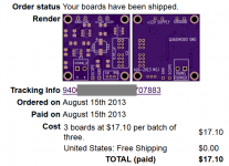
I ordered Quasimodo V.3 SMD boards from two different fab houses: OSH Park, and Seeed Studio. Google can find their websites for you. I have attached my invoices below, so you can see how much I paid.
I ordered the minimum quantity (3 boards) from OSH Park, and paid (17.10 / 3) = $5.70 per board including shipping to USA. Yes the boards really are purple and yes the solder pads really are gold ("ENIG"). That's OSH Park's signature, their emblem.
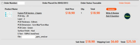
I ordered twenty boards from Seeed Studio (their minimum quantity is 10), and paid (25.50 / 20) = $1.28 per board including shipping to USA. These boards are the more conventional green color, and the pads are the more conventional tinned solder ("HASL") finish; you can see photos of them in post #27 above.
After performing my own Quasimodo experiments, I had zero OSH Park boards left over, and 12 Seeed Studio boards left over. The ones I sold here were Seeed Studio boards. (Why did I ask $5.00 for a $1.28 board? To pay for the bubble-padded envelope and for postage.)
Lots and LOTS of microcomputer hobbyists, MIDI hobbyists, and audio hobbyists use these two board houses, and there are tons of reviews of them online. You can get the opinions of many people, about quality and solderability of each fab house's boards. In my opinion, both were quite good and I had no problems with either one. If you decide to send the Quasimodo Gerber files (post #22) to either of these fab houses, I think the results will be satisfactory.
But remember, Quasimodo is a test-jig idea; you can implement that idea however you like. You don't need a PCB (proof: see post #18), you don't need surface mount components, and you don't need to copy my schematic. It's just a digital circuit: it's just a square wave oscillator. Have some fun! Slap together your own design (hint: there is a model of the 555 timer chip in LTSPICE's library named "misc"), simulate it, get it working in simulation, then build it on a piece of StripBoard or Vero Board or plywood. Have some fun! This is a hobby; it's supposed to be fun.
Attachments
Yes the V.3 SMD Quasimodo board does have C3 = 150 nF soldered straight onto the board. That's because I wasn't able to lay out a minimum-cost PCB (less than 5cm X 5cm) with sockets for all three of C2 and C3 and RV1. Perhaps your PCB layout skills are better than mine; maybe you'll succeed where I did not.
However, fixing C3 at 150nF is not a problem for the 3-element CRC snubbers that I prefer. Every transformer I've connected to Quasimodo V.3 SMD has found an optimum (zeta = 1.0) snubber using C2 = 10nF, C3 = 150nF, RV1= variable. Member Karsten Sømand has made the same discovery: C3=150nF successfully snubs all the transformers he has tested with his Quasimodo, to zeta = 1.0.
The people who might be more likely to want an adjustable C3, are the ones who insist upon using 2-element snubbers rather than 3-element CRC snubbers; see the design note pp. 12-13. For these folks, the secondary "characteristic impedance" is likely to be 3X to 10X larger than the characteristic impedance with a CRC snubber. So the optimum Rsnub will similarly be 3X to 10X larger than the optimum R in a 3 element snubber. If that is the case, they may ask themselves: why "waste" money on a 150nF capacitor C3 when a 15nF (or possibly even 1nF) cap might do the job? And so they'll want a socketed C3.
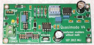
One obvious way to get a socketed C3 is to bite the bullet and lay out a larger PCBoard. In fact, that's what I've done for Quasimodo V.4 (thru-hole components). It fits within Seeed's second-cheapest boardsize constraint: less than 5cm X 10cm. But V.4 isn't back from fab yet and I haven't put it through verification testing. There might be a layout error or a circuit design error.
However, let me emphasize: Quasimodo V.3 with fixed C3=150nF, successfully tested and optimized snubbers for every single one of the transformers I connected to it. I don't own any transformers for which V.3 can't do the job, and for which I must wait until V.4 arrives. Nor am I aware of any other Quasimodo owner who has found that C3=150nF prevents him/her from performing all desired tests.
If you're still nervous about this, maybe you should start by building your Quasimodo on a solderless breadboard as shown in post #18. Now all components of Quasimodo are socketed, and you can change them out however you please. Connect it up to some transformers and fool with it, for two or three lab sessions. See whether you actually do need different values of C3. If you do, provide a socket for it on your PCB layout. If you don't, maybe Quasimodo V.3 SMD's Gerber files in post #22, are adequate for your needs.
After you look at the board layout, maybe you'll conclude that the socket I provided was ridiculously oversized (0.2 x 0.8 inches? really??), giving excessive "flexibility" that simply isn't needed. If the socket is made smaller, perhaps 2 of them will fit.
However, fixing C3 at 150nF is not a problem for the 3-element CRC snubbers that I prefer. Every transformer I've connected to Quasimodo V.3 SMD has found an optimum (zeta = 1.0) snubber using C2 = 10nF, C3 = 150nF, RV1= variable. Member Karsten Sømand has made the same discovery: C3=150nF successfully snubs all the transformers he has tested with his Quasimodo, to zeta = 1.0.
The people who might be more likely to want an adjustable C3, are the ones who insist upon using 2-element snubbers rather than 3-element CRC snubbers; see the design note pp. 12-13. For these folks, the secondary "characteristic impedance" is likely to be 3X to 10X larger than the characteristic impedance with a CRC snubber. So the optimum Rsnub will similarly be 3X to 10X larger than the optimum R in a 3 element snubber. If that is the case, they may ask themselves: why "waste" money on a 150nF capacitor C3 when a 15nF (or possibly even 1nF) cap might do the job? And so they'll want a socketed C3.
One obvious way to get a socketed C3 is to bite the bullet and lay out a larger PCBoard. In fact, that's what I've done for Quasimodo V.4 (thru-hole components). It fits within Seeed's second-cheapest boardsize constraint: less than 5cm X 10cm. But V.4 isn't back from fab yet and I haven't put it through verification testing. There might be a layout error or a circuit design error.
However, let me emphasize: Quasimodo V.3 with fixed C3=150nF, successfully tested and optimized snubbers for every single one of the transformers I connected to it. I don't own any transformers for which V.3 can't do the job, and for which I must wait until V.4 arrives. Nor am I aware of any other Quasimodo owner who has found that C3=150nF prevents him/her from performing all desired tests.
If you're still nervous about this, maybe you should start by building your Quasimodo on a solderless breadboard as shown in post #18. Now all components of Quasimodo are socketed, and you can change them out however you please. Connect it up to some transformers and fool with it, for two or three lab sessions. See whether you actually do need different values of C3. If you do, provide a socket for it on your PCB layout. If you don't, maybe Quasimodo V.3 SMD's Gerber files in post #22, are adequate for your needs.
After you look at the board layout, maybe you'll conclude that the socket I provided was ridiculously oversized (0.2 x 0.8 inches? really??), giving excessive "flexibility" that simply isn't needed. If the socket is made smaller, perhaps 2 of them will fit.
This may be silly, but I actually asked to account for possible tolerance on capacitance.
For example, let's say I use the V.3 Quasimodo to snub a secondary. I socket a 10nF cap and 471R is say the optimal.
Now, say for example the C3 cap on Quasimodo was actually 155nF on a 5% tolerance and the cap inserted a 9.8nF on 5% too.
When I solder these components on my application, I will solder a 150nF that, assuming a 5% tolerance, could be anywhere from 142.5nF to 157.5nF. So the optimal snubbing resistor could not be 471R, but another value.
My intuition is that it will not matter at all and snubbing will be adequate. Just wondered whether there is some precaution already taken - for example, maybe you have concluded that a 150nF with 5% tolerance for this given resistor will alter ζ between, say 0.93-1.07 (random numbers), so snubbing is still adequate.
Do you think all this is worth considering?

<<Just curious. Couldn't one simply use a signal generator and audio power amp to drive the signal into the transformer? Many of us have those handy around the shop.
Sure can, but like Hagerman that leads to a fair bit of math to crunch to determine values after you find the resonant frequency. Much easier and faster to find the snubber value empirically with the actual Cx and Cs you intend to use.
And in my case at least, probably more accurate given a misspent youth and a midlife penchant for good red wine!
Johno, I just thought (being hasty? maybe) that C3 would be the injection capacitor that sets the frequency of the ringing, so it could have a more severe impact on the snubbing, since the resistor would be chosen to damp the ringing "formed" by C3. I read the application note again and realised that this is a task designed for C2, that is socketed. ")
Couldn't one simply use a signal generator and audio power amp to drive the signal into the transformer? Many of us have those handy around the shop.
Sure. If you want to replicate the Quasimodo idea, the testbench audio amp will be the piece which provides an ultra low output impedance. The signal generator produces an 0.5V peak-to-peak square wave @ 120Hz, that you feed into the testbench audio amp. The audio amp has a voltage gain of ~ 20X, so the amp's output drives the injection capacitor Cx with a 10V peak-to-peak square wave. Cx drives (C3 + Rs) and the transformer secondary, replicating the Quasimodo topology. Just make sure the power amp has sufficient bandwidth to give < 30 nanosecond rise time (in this case: fall time!) on the square wave's edges.
Using the good old Risetime - Bandwidth equivalency relationship: (tr * BW = 0.34), that means you need a testbench audio amp with bandwidth > 11.3 MHz. Mind you, this is the required bandwidth at a gain of 20X. The Unity Gain Crossover Frequency (where the OPEN LOOP amplifier's Bode plot crosses Av=0 dB) needs to be > 220 MHz.
If your testbench audio amp's bandwidth isn't this high, you won't be able to test out 2-element snubbers such as the ones advocated in Morgan Jones's article in Linear Audio volume 5. Because 2-element snubbers use a very tiny Cx, they have a very high ringing frequency omega_n (QM note equation A-10). Your square wave edge stimulus (that squirts out of your testbench audio amp) needs to be even faster.
However, you probably will be able to test out 3-element CRC snubbers such as the ones discussed in the Quasimodo note. Do a rough calculation of your transformer's omega_n, including the Cx you plan to use. Then make sure your testbench audio amp's bandwidth is higher than this.
(Perhaps you've noticed that equations and calculations are involved in this signal_gen + bench amplifier approach. Some people are perfectly happy with equations and calculations; others prefer "no-math" methods of skinning the cat.)
Last edited:
This great, as a lazy engineer I love the empirical measurement approach.
How is Version 4 coming along? Will you post the PCB and BOM files? I will be building this but given my arthritic hands and near 70 year old eyesight I would prefer a real world through hole component versus the Gullivers Lillipution SMD version.
How is Version 4 coming along? Will you post the PCB and BOM files? I will be building this but given my arthritic hands and near 70 year old eyesight I would prefer a real world through hole component versus the Gullivers Lillipution SMD version.
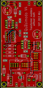
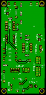
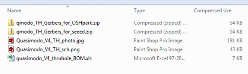
I've attached the Gerber files and a Bill of Materials for a thru-hole implementation of the Quasimodo idea. They are in a .zip archive, attached to this posting. So far, I have built two of these boards and they work quite nicely. A component side plot is displayed in red (below), back side plot is green.
If anyone wants to organize a group buy for a batch of these boards, and/or boards + kits of parts, please do so with my blessings. The BOM and the CAD files are right here.
Edit The attachment here is incomplete. For the full attachment, see post #58"
If anyone wants to organize a group buy for a batch of these boards, and/or boards + kits of parts, please do so with my blessings. The BOM and the CAD files are right here.
Edit The attachment here is incomplete. For the full attachment, see post #58"
Attachments
Thank you.
Do you have gerber files for the boards?
Demonstrating my lazy engineer attitude what are the dip switch conbinations versus frequencies and what do you suggest regards the use of those frequencies to arrive at the best snubber component compromise?
You have been very generous with your time and skills so I feel quilty asking these questions.
Again thank you very much.
... Do you have gerber files for the boards?
I've attached the Gerber files ... they are in a .zip archive, attached to this posting {#54}
I recommend you compare the schematics of V3 and V4, they are attached to post #1 in this thread. One includes a DIPswitch and the other does not. I recommend you start out your Quasimodo adventures with your DIP switches set in such a way that your board exactly mimics the switch-free V3. After a couple hours of experimentation in pure V3 mode, it's time to horse around. Flip some switches at random, and see if things get better or worse, in your opinion. Don't worry, you can't hurt anything. None of the 2^4 = 16 possible settings of the DIP switches, are harmful.
I will leave it up in the air, as a slight mystery: Why might it be useful to have different oscillator frequencies? diyAudio members may enjoy thinking about this and possibly posting their guesses. As soon as someone chimes in to say "Hey! I've actually BUILT one of these (here's a photo) and I need someone to tell me where to set the switches and why! Don't worry, you can't hurt anything is NOT very reassuring!" ...
As soon as someone says that, and shows a picture of their QM, I'll post my original reason(s) why I included the DIP switches. By then, another member may have suggested another reason that's even better than my own.
Thank you again.
The zip file contained a schematic, a BOM and a picture of the loaded board I didn't see gerber files in there.
I will build one as soon as I can, and look forward to exploring the effect of different frequencies. Obviously I need to re-read the thread carefully, I skipped through it too quickly.
Unfortunately I'm going to be away from home until early December, building up my SWMO brownie points with a cruise, should buy me at least six months of indulgence.
Regards
Mike
- Home
- Amplifiers
- Power Supplies
- Simple, no-math transformer snubber using Quasimodo test-jig