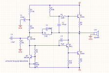
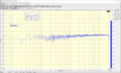
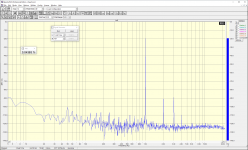
Ok did some more testing with a simple Vbe multiplier to try taming the wild offset. I tried placing Q5 on various points on the heatsink and even directory on top of one of the output transistors. It doesn't seem to match the coefficient of the output devices but that's not surprising. What is surprising is how it effects the THD.
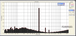
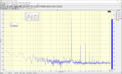
680 ohm resistor 0.2%,
Vbe with MP26 (PNP) 0.55%
Vbe with MP10 (NPN) 2%
Why does this simple ccs add so much distortion? Also interesting that the distortion is mostly second harmonic.
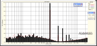
680 ohm resistor 0.2%,
Vbe with MP26 (PNP) 0.55%
Vbe with MP10 (NPN) 2%
Why does this simple ccs add so much distortion? Also interesting that the distortion is mostly second harmonic.
Attachments
I can't say anything about this. Everything needs to be well researched. Still, it would not hurt to replace the MP10 with a silicon transistor. The deviation of the "zero" voltage at the output should be more stable. The author got such a THD.Why does this simple ccs add so much distortion?
1. 1 kHz, 1 V, 8 ohms;
2. 1 kHz, 6 V, 8 ohms.
Attachments
Interesting patent.
Did some reading on the JLH class A update site https://sound-au.com/tcaas/jlhupdate.htm and decided to implement their two transistor current source and it works great! THD is just as low (if not lower need more testing) than a resistor.
I don't understand why replacing the first transistor with silicon would help with offset drift. It draws 2ma and only heats up from the surroundings. The middle transistor is what really makes the difference. A small heatsink does help, but the designs from post #588 seem to agree.
Try to replace the first transistor with a silicon one and you will be very surprised.I don't understand why replacing the first transistor with silicon would help with offset drift.
Only it will be necessary to change the bias on the first transistor, since the germanium transistor opens at 0.3 V, and the silicon one - 0.7 V. 😉
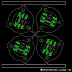
Thought someone could make use of these files. Those large transistors require a clamp to hold them to the heatsink. Mounting multiple transistors on the same heatsink can be a problem because of the metal clamp. Here are step and dxf files for anyone wishing to 3d print or laser cut some clamps from plastic. Now you can put a thermal pad under the transistor and clamp them down without anything shorting. Is there a proper name for this particular package?
Attachments

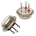

In the USSR it was called a flange ( фланец ) ...... Is there a proper name for this particular package?
You can do it, but the plastic must be durable and 3 ... 5 mm thick. These are clamping washers (flanges). We ordered the same ones in China, but for installing diodes as a temperature sensor.Here are step and dxf files for anyone wishing to 3d print or laser cut some clamps from plastic. Now you can put a thermal pad under the transistor and clamp them down without anything shorting. Is there a proper name for this particular package?
Attachments
Because it is not a current source but a voltage source. It is a vbe multiplier! 😳Ok did some more testing with a simple Vbe multiplier to try taming the wild offset. I tried placing Q5 on various points on the heatsink and even directory on top of one of the output transistors. It doesn't seem to match the coefficient of the output devices but that's not surprising. What is surprising is how it effects the THD.
680 ohm resistor 0.2%,
Vbe with MP26 (PNP) 0.55%
Vbe with MP10 (NPN) 2%
Why does this simple ccs add so much distortion? Also interesting that the distortion is mostly second harmonic.
RE the "germanium triode" experiment mentioned sometime ago: Firstly, the linked article is not clear on how exactly they connect the DUT (for the first, "not nice" set of curves, they say "a PNP transistor gets simply used as NPN transistor", while for the triode-like curves they say "take a ... PNP Transistor, connect it simple reverse, so as NPN Transistor" :-/). I tried the various combinations, and the one where "simply" the collector and emitter are switched does indeed result in triode-like curves... for any transistor, even silicon ones, and you can easily simulate that in Spice:
View attachment 1024674
(P210 is a germanium PNP, [2S]A1186 is silicon; disregard the MOSFET-related stuff - that was just a hack to make the Peak tester do voltage drive instead of current drive.)
View attachment 1024675
I think early guitar fuzz effects used germanium trz like that.
I may be wrong (I often am :-D), but aren't these just the Vbe vs. Ic curves, offset by the base voltage source step? Meaning there's no practical triode-like behaviour as such...?
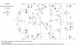
 I calculated and tested when I stuffed the PCB
Found germanium treasure 🙂
https://www.diyaudio.com/community/...-do-with-this-transistor.399566/#post-7357346
https://www.diyaudio.com/community/...-do-with-this-transistor.399566/#post-7357346
Hi So You think that they connected DUT (ASZ16, PNP Ge Transistor)RE the "germanium triode" experiment mentioned sometime ago: Firstly, the linked article is not clear on how exactly they connect the DUT (for the first, "not nice" set of curves, they say "a PNP transistor gets simply used as NPN transistor", while for the triode-like curves they say "take a ... PNP Transistor, connect it simple reverse, so as NPN Transistor" :-/). I tried the various combinations, and the one where "simply" the collector and emitter are switched does indeed result in triode-like curves... for any transistor, even silicon ones, and you can easily simulate that in Spice:
View attachment 1024674
(P210 is a germanium PNP, [2S]A1186 is silicon; disregard the MOSFET-related stuff - that was just a hack to make the Peak tester do voltage drive instead of current drive.)
View attachment 1024675
I may be wrong (I often am :-D), but aren't these just the Vbe vs. Ic curves, offset by the base voltage source step? Meaning there's no practical triode-like behaviour as such...?
As You draw O1 NPN 2SA1186
That is for "positive grid bias" voltages at the base to gnd?
.
But they said that reverse PNP normal opperation to NPN device
Did They just reverse power supply to already right connected NPN device, leaving the Vbe as PNP positive values,
OR
revert the polarity of Vbe to negative values?
.
Thanks 🙂
.
I am asking that beacuse i made some spice model BUT for negative values from 0 with increment of -2V.
That is as classic triode WITH negative grid bias...
.
On the picture stated Vert square 10mA, horizontal square 2V, step 2V,
All values are positive at least on the display, no datas what the first value for stepping?
BUT if they are used positive values, that model obviously NOT valid...
.
I will check it out with the positive values of Vbe as Ug for positive grid bias
As I said, their explanation of how they connected the DUT was not clear to me at all, so I just kept switching the test leads until I got the triode-like curves. If that particular connection is also what they did, I dunno. And if this connection has any practical use to achieve triode-like amplification, I've no clue either... 
- Home
- Amplifiers
- Pass Labs
- Germanium investigations