though, bummer, disclaimer
for this tweak , to work , difference between Ugs of SIT and Ugs of Mos must be , say , 1V35 at least ....... so we have enough voltage space to squeeze Darlington in
you can easily check that on your Sissy - just measure voltage between gates of SIT and Mos
Fairchild and I think the ON Semi FQA P-channel parts have VGS in the 5.7V range.
Maybe my delay in finishing my SissySit will cause a benefit here! Can't wait but will be a month or so before I have a chassis anyway...
Russellc
Russellc

The darlington allows for more current, does that make the Sit reach it’s equilibrium faster?
The darlington allows for more current, does that make the Sit reach it’s equilibrium faster?
point is keeping same resistor values going from rails to gates,keeping Rin high enough.... so no change in current
Let's present and explains some ..... 🙂
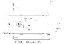
See attached - simplified schm of amp , biasing mech
Hall Isense chips are sitting in da rails , sending Isense to optocoupler's LED
when Iq is rising , LED is shining more , thus opening optocoupler's bjt more , enabling more current through Rup and Rdown , thus squeezing space/voltage between Gsit and Gmos nodes, thus closing them and decreasing Iq
same opposite function for opposite change of Iq
3m3 cap is there to prevent abrupt changes in function , ignoring anything resulting from modulation (playing da music)
limiting/important factor is that we need at least Vbe (PN voltage drop) between Gsit and Gmos nodes , for circuit being able to function ....... so we must choose (or be lucky enough ) to have SIT with smaller Vgs than Mos Vgs for at least that amount , and little more
Vbe being 0V65 (or 0V7 for some) , we are shooting for at least 0V85 or 0V9 , for better sleep
Attachments
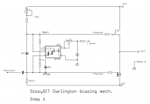
Darlington Opto , Step 1
problem is there -when we have nicely behaved Mos and VFet , Iq is creeping with temperature some , also DC offset ( Rup and Rdown are not of same value ad can't be of same value) but amount of that is acceptable and everything is good in Temp Equilibrium
however, in cases where we have some lesser behaving Vfet ( or mos?) , showing some gate leakage or what , some Greedy Boyz informed that Iq creep is somewhat unsettling ; conclusion is that we simply need more gain in biasing mech. , while still having decent and non-surprising behavior in both Temp and Vrail changes domains ; believe me - tricky to ensure all that in same time , when you are dealing with inherently not symmetric circuit
we all know M2 , as origin of this approach ........ but there biasing mech. is dealing with easy and predictable task - upper and lower gates are close in value and opposite in sign , entire shebang is sorta symmetric , Rup and Rdown are close enough that DC offset is inherently stable even with slight changes in Iq
Indra ( who else?) mentioned sometime ago that there is 6N139 opto - with Darlington bjt pair in output ; he even posted small sim but bummer was that behavior of his arrangement was extremely erratic , taking in account changes in temperature and Vrails ........ simply too much gain
so , after some time , I came to this arrangement, see attached pic.
it's pretty straightforward ....... 2 resistors and cap more , besides change of opto
lower resistor is base resistor for 2nd bjt in Darlington , while upper resistor is colector resistor for 1st darlington bjt , to control gain of circ .... in fact , both of them are directly involved
little cap is to prevent abrupt changes in action of second darlington bjt ; it serves same purpose as 3m3 between gate nodes , but on previous level
Attachments
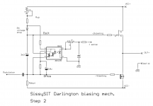
same, Step 2
OK , I made entire shebang on the fly ( forgot to take pic, will later) and everything was rooooosy ......... and I even posted some info , even without 100% established values for these 2 resistors .... that needs some time , every change needing complete cool-down and heat-up cycle , to check behavior
then I realized a problem - Darlington is needing 2Vbe (2xPN) space to function properly !
Oh Boy - whic means not covering at least 40% of cases , regarding difference between Gsit and Gmos voltages

OK, whatever ...... rushing from workshop , due to some other things I had in last few days to do , after some 5mins or so , I came to solution ...... moving 1st darlington collector outa Gsit-Gmos window ........ so leaving just 2nd darlington bjt in it
it was easy , once you get an idea ; ( ideas are those things making things easy and life interesting , in general)
solution is one simple 1N4148
see attached
OK , I made entire shebang on the fly ( forgot to take pic, will later) and everything was rooooosy ......... and I even posted some info , even without 100% established values for these 2 resistors .... that needs some time , every change needing complete cool-down and heat-up cycle , to check behavior
then I realized a problem - Darlington is needing 2Vbe (2xPN) space to function properly !
Oh Boy - whic means not covering at least 40% of cases , regarding difference between Gsit and Gmos voltages
OK, whatever ...... rushing from workshop , due to some other things I had in last few days to do , after some 5mins or so , I came to solution ...... moving 1st darlington collector outa Gsit-Gmos window ........ so leaving just 2nd darlington bjt in it
it was easy , once you get an idea ; ( ideas are those things making things easy and life interesting , in general)
solution is one simple 1N4148
see attached
Attachments
all in one place
so , I'll need day or two to finish tests for final resistor values , but for now there is 3K3 up and 6K8 down ;
once when I'm done , will post short and sweet piccie tutorial how to conduct that small conversion
to recapitulate , for now - change of one resistor value ( R15 , that one preceding trimpot on opto LED side) , two more resistors , one 10uF/16V elco (even 6V3 one will do the job) , one 6N139 , one 1N4148 in case that gates of your SIT-Mos pair are too close
anyway , sch with preliminary values is :
(last but not the least - Indra is Da Man 🙂 )
Attachments

Last edited:
Gate leak will develop voltage across R21 (sit flying gate stopper), reducing to something like 39-68R could help on less severe ones.
of course , but better safe than sorry
there is one thing I'm constantly forgetting to pursue - trying to find nice little adequate inductance , to use them instead of gate resistors
plenty of these nice through hole and smd ones , but remembering to order some and test is trickiest
there is one thing I'm constantly forgetting to pursue - trying to find nice little adequate inductance , to use them instead of gate resistors
plenty of these nice through hole and smd ones , but remembering to order some and test is trickiest
it was easy , once you get an idea ; ( ideas are those things making things easy and life interesting , in general)
solution is one simple 1N4148
see attached
It seems to happen quite regularly doing a number 2 on the toilet.
Hahaha
So beautiful.
Thanks to the idea generator (pooing on the toilet). Well at least that’s how it works for me.
Hahaha
Thanks to the idea generator (pooing on the toilet). Well at least that’s how it works for me.
Hahaha


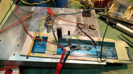
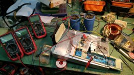
OK , testing of R2 are done
behavior , after everything set in temp. equilibrium (set to Iq 1A8 , DC Offset ~0mV):
-cold start : Iq 2A02 , DC Offset +70mV
-stability in temp. equilibrium against mains (rails) fluctuation :
-10% mains , DC Offset +170mV , Iq 1A74
+10% main , DC Offset -150mV , Iq 1A87
so , silly thing is now having negative TempCo (difference between cold and hot)
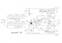
I made new , final schmtc - attached
parts of interest are - change of value of R15 (ref. original pcb , so no worries) , two additional resistors , on this new schmtc marked as R13 and R14 ......and one additional diode - marked as D3..... and one tiny 10u cap (C13)....but do not worry about that ("new") too - pic tutorial follows these days , showing how to do simple
conversion on existing pcbs , with existing parts nomenclature
behavior , after everything set in temp. equilibrium (set to Iq 1A8 , DC Offset ~0mV):
-cold start : Iq 2A02 , DC Offset +70mV
-stability in temp. equilibrium against mains (rails) fluctuation :
-10% mains , DC Offset +170mV , Iq 1A74
+10% main , DC Offset -150mV , Iq 1A87
so , silly thing is now having negative TempCo (difference between cold and hot)
I made new , final schmtc - attached
parts of interest are - change of value of R15 (ref. original pcb , so no worries) , two additional resistors , on this new schmtc marked as R13 and R14 ......and one additional diode - marked as D3..... and one tiny 10u cap (C13)....but do not worry about that ("new") too - pic tutorial follows these days , showing how to do simple
conversion on existing pcbs , with existing parts nomenclature
Attachments
Last edited:
- Home
- Amplifiers
- Pass Labs
- Babelfish M25, SissySIT - general building tips and tricks