All the IRFP260s I have on hand are the original IR parts, bought as NOS. Things may be a trifle different now that Vishay, Infineon. and Ixys are making the part. There may be others in the game. too. All the parts I looked at had the same 0.5 degreeC/Watt junction to case thermal resistance. This means that if you blow ten watts in the part, the chip inside will have a 5C differential with the device case. This is pretty good for a cheap fet. If I remember correctly, the Ixys part has a thermal resistance of about half this, indicating that there is a huge die inside. This is also borne out by the enormous gate capacitance (~ 6 nF, if I remember correctly).
All the IRFP260s I have on hand are the original IR parts, bought as NOS. Things may be a trifle different now that Vishay, Infineon. and Ixys are making the part. There may be others in the game. too. All the parts I looked at had the same 0.5 degreeC/Watt junction to case thermal resistance. This means that if you blow ten watts in the part, the chip inside will have a 5C differential with the device case. This is pretty good for a cheap fet. If I remember correctly, the Ixys part has a thermal resistance of about half this, indicating that there is a huge die inside. This is also borne out by the enormous gate capacitance (~ 6 nF, if I remember correctly).
how many Watts can get from IRFP260 this circuit ?
Regards
Thiago
http://www.mouser.com/ProductDetail...6sg/T%2b0bHb8btWkzppYmXDJimkDLSWtBhyDJVkpTg==
Low voltage high current was a favorite back in the day. What changed?
Low voltage high current was a favorite back in the day. What changed?
For our nefarious purposes here, I don't pay as much attention to the raw volts and amps rating of the part, as we're not really exercising that capability in the slightest. The real indicator of utility (assuming you're not violating any other rating) is the theta jc of the part, or its junction to case thermal resistance. This number dictates the amount of power you can blow through a part for a given temperature rise, a pressing concern for a Class A design. A part with theta JC of 1 degree per watt will have a temperature differential between die and case of 1 degree C per Watt dissipated. This is a fairly so-so rating. The IRFP260 has a theta JC of 0.5 degrees/Watt, which is pretty good. The monster Nelson/IXYS part has a theta JC of 0.25C/Watt, which not only indicates a large area die, but meticulous attention to the thermal interface between die and case, as the case is isolated. An Aluminum Nitride pad is used for isolation, a material with superb thermal characteristics.
Edit - the IXYS part has a gate capacitance of 8 nF (not 6), which indicates a really huge die area with corresponding power dissipation capability.
Edit - the IXYS part has a gate capacitance of 8 nF (not 6), which indicates a really huge die area with corresponding power dissipation capability.
Last edited:
Papa say on video BAF " is worst the efforts ".....Next step i need huge psu transformers for planed monoblocks.
How is minimum transformer VA ratio for 50 watts rms = 600 VA mono ok ?
After study of Mr Pass article :
https://www.passdiy.com/project/articles/power-supplies
for no compromise pure class A 200 watts amplifier we need 3000 watts toroid donut.
For 50 watts is 50 x 15 = 750 watts toroid transformer is minimum rate no less.
I was short with 600 VA....

Hi Gior and DiyersIf I understand well the article he means 3kW for both 200W channels together; in this case your 600VA looks enough
We need clarify : toroid minimum power rate for each mono block &
toroid with two secondaires for equivalent power stereo amplifier ??
Example for 200W pure class A amplifier toroid minimum is 3kW power rate with two secondaires who deliver 1,5kW each
or is 2x 3kW so give power rate is for simple secondaire output
or total of two's


For single-ended 50 watts no compromisse class A mono block minimum toroid power rate with only one secondaire is ?
Answers is welcome
Have a nice day
Papas 50W single ended class A "Schade feedback amp" presented at BAF 2015 consumes a continuous 192Watts (60V B+ x 3.2A bias current).
If a understood Papas reasoning in the paper about power supplies he states that the transformer should have a rating of at least three times the continuous power consumption. 600VA should do for a 50W monobloc.
If a understood Papas reasoning in the paper about power supplies he states that the transformer should have a rating of at least three times the continuous power consumption. 600VA should do for a 50W monobloc.
Re question from post 222.
If you have a design with modulated topside current source and things are set just right, you can get 2X the current in one driver, just as the other side bottoms out to zero. Assuming that this really can be done with the design, and the rail voltages are set just right, you theoretically can get an output power roughly equal to Pdmax, the max dissipation in one driver. Assuming you have equal dissipation in each output device, this sets the overall efficiency at ~50%, which is the max for a class A design. If the topside current source is not modulated, the power capability goes down to ~0.5 Pdmax, or an overall efficiency of 25%. All this can be derived with nothing more esoteric than Ohm's law.
The allowable power dissipation will depend on device characteristics and the thermal interface. For a good heat sink, I think that an IRFP260 could support 40W dissipation. This is assuming a Tj max of 100C.
I'll do some thinking about what this actually means for a thermal interface with a max ambient of, say, 40C, to test the validity of the 40W assumption, and report back.
on the subject of heat dissipation and cooling: I built several amps using a quiet pwm Noctua fan.
http://www.diyaudio.com/forums/pass-labs/201281-burning-amp-ba-3b-balanced-57.html#post4794952
for that matter I developed (with a lot of help from a friend of mine) a control board which runs the fan based on temp feedback, also provides soft start, speaker disconnect for amp on/off thump, turn on by an auxiliary switch from the preamp, and has a speaker protection function built in but not tested. for the the latter I just did not have the time to play with it to verify the function and fine-tune the schematic values. Other than that I have three of these boards already in my amps working fine.
If there is a volunteer to fine tune the speaker protection part of the circuit I will make available a prototype pcb with a flashed controller. If you are capable of PIC Basic programming I will also give you the software.
This is only for the more experienced with a history of contributing on the forum since I am not looking to give up the board for under the cost for somebody to just plug it in and use as is; the idea is to help finish the development as the speaker protection on the board should theoretically work but it takes someone to put in the time to play with the settings.
You will still have the cost of all the parts to populate the board and buy the Noctua fan, so I imagine you would want to use the board in your finished amp. Please let me know if interested.
Last edited:
Re question from post 222.
If you have a design with modulated topside current source and things are set just right, you can get 2X the current in one driver, just as the other side bottoms out to zero. Assuming that this really can be done with the design, and the rail voltages are set just right, you theoretically can get an output power roughly equal to Pdmax, the max dissipation in one driver. Assuming you have equal dissipation in each output device, this sets the overall efficiency at ~50%, which is the max for a class A design. If the topside current source is not modulated, the power capability goes down to ~0.5 Pdmax, or an overall efficiency of 25%. All this can be derived with nothing more esoteric than Ohm's law.
The allowable power dissipation will depend on device characteristics and the thermal interface. For a good heat sink, I think that an IRFP260 could support 40W dissipation. This is assuming a Tj max of 100C.
I'll do some thinking about what this actually means for a thermal interface with a max ambient of, say, 40C, to test the validity of the 40W assumption, and report back.
thank you so much.
I will follow , because I have many irfp260 in the drawer
Regards
Thiago
OK
The problem appears to be acceptable heat sink temperature rather than device junction temperature, Given a 0.5C/W theta JC for the IRFP260 and a 40W dissipation for each device, the junction of each device will be sitting at a 20C differential above the case temperature. This means that in order to satisfy the 100C max junction temperature the case temperature must be below 80C. Even considering a relatively mediocre device to heat sink interface, the heat sink temperature will be quite high.
Working this backwards, one would ideally like to have heat sinks that will not raise blisters when touched. This means a heat sink temperature of 60C or below. That's still "OW" temperature, but not an immediate burn/blister situation. Assuming a max ambient temperature of 40C (not all that stringent), this gives you a 20C temperature rise over ambient for 80W total dissipation (one heat sink per channel). That's 0.25C/W thermal resistance - a largish heat sink, but still doable. If one uses air or liquid cooling, the heat sinks can shrink considerably. A little air can go a long way. A 60C heat sink temperature will result in a device junction temperature of somewhere between 90 and 100C, depending on the device case to heat sink thermal resistance. Given what I see here, I stand by the 40W/device estimate, though I wouldn't push it any higher for a convection cooled heat sink.
Edit - I did some nosing around, and it looks like 12-16 in. of Heat Sink USA's 10.08 in extrusion would do the trick (0.8C/W for 3").
Last edited:
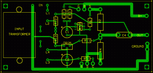
PCB for scaled down version
Hello
Hereafter a PCB for a scaled down version of the "Schade BAF2015" amp.
It refers to the schematic drawn by Generg and shown in post #564 BAF2015 coverage.
Input transformer in this case is a Jensen with wire leads.
As i am prone to produce errors, the layout may include some. Corrections are most welcome.
Changes can be made after unzipping with the software Express PCB.
Have a nice day
Attachments
Last edited:

Hello
Hereafter a PCB for a scaled down version of the "Schade BAF2015" amp.
It refers to the schematic drawn by Generg and shown in post #564 BAF2015 coverage.
Input transformer in this case is a Jensen with wire leads.
As i am prone to produce errors, the layout may include some. Corrections are most welcome.
Changes can be made after unzipping with the software Express PCB.
Have a nice day
I haven't checked for errors, but either way very nice work mate.
- Home
- Amplifiers
- Pass Labs
- 50w Single-Ended BAF2015 Schade Enabled