Did I ruin something?
Probably...... not...
")
You first need to do three checks.
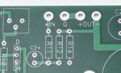
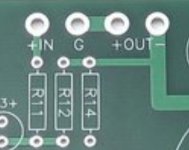
1/ We always need to confirm the supply voltage is present and correct. Measure from ground to the centre leg of power FET Q2. Be very careful not to short the legs with the meter probe. Confirm the 24 volts is present.
2/ Check the voltage on the middle leg of power FET Q1. It should be approx 12 volts.
3/ Check the FET's are running hot (they should) and that there is approximately 0.9 volts across the series/parallel combination of R1 to R4. In other words from the centre (Drain) of Q1 to the rightr hand (Source) leg of Q2 as viewed looking down on the device.
Those checks show the amp is basically OK.
Make sure you have the speaker connections from board to socket correct. Remember the output of the amp is actually wired to the negative terminal and ground to the positive.
Make sure the input socket centre pin has continuity to one end of R11.
Thanks for your response. My multimeter went bad and I had to get a new one. I went through the checklist and came up with the following. #1, right side = 23.9v, right side = 23.9-24v. #2, right side 7.7 drift to 13 drift back to 8.2, left side 11.6 drift down to 7.6 then steadied at 7.9v. #3, right .8v, left .8 to .9. Checking for continuity. I'm not sure I did this correctly but from the center pin of the input, right side to
the leg of R11(closest to the edge of the board) I had continuity, but switching to the leg close to the center of the board for R11, no continuity. Left side, no continuity from input center pin to either leg of R11, no continuity. Checking the tempereature of the FET's with a Thermapen I got 95F for Q1's and 109F for Q2's after about 10 minutes.
I have attached pictures of my assembly. You will immediatel note that the parts soldered to the board are elevated off the board. After watching many youtube videos of the build a couple recomended doing that. I have no idea why or even if it is a valid idea.
I am open criticism and suggestions.
Thanks, Dave


.jpg")

.jpg")
the leg of R11(closest to the edge of the board) I had continuity, but switching to the leg close to the center of the board for R11, no continuity. Left side, no continuity from input center pin to either leg of R11, no continuity. Checking the tempereature of the FET's with a Thermapen I got 95F for Q1's and 109F for Q2's after about 10 minutes.
I have attached pictures of my assembly. You will immediatel note that the parts soldered to the board are elevated off the board. After watching many youtube videos of the build a couple recomended doing that. I have no idea why or even if it is a valid idea.
I am open criticism and suggestions.
Thanks, Dave
Easy one first. Lifting parts is often done for ventilation around the part. Apart from the power FET's the ACA runs cold but what you have done will cause no problems at all.You will immediatel note that the parts soldered to the board are elevated off the board. After watching many youtube videos of the build a couple recomended doing that. I have no idea why or even if it is a valid idea.
#1, right side = 23.9v, right side = 23.9-24v. #2, right side 7.7 drift to 13 drift back to 8.2, left side 11.6 drift down to 7.6 then steadied at 7.9v. #3, right .8v, left .8 to .9.
#2 is the big standout problem. #1 and 3 look fine.
Over what time period is this drift? Is it slow (several seconds or longer) or just a couple of seconds?
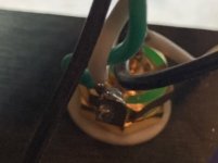
The soldering on the FET's looks a bit flaky tbh
Use a hot iron with a decent sized tip and apply solder and the iron together to make a large clean shiny joint. If I was building an ACAS I would solder both sides of the board. If the iron is hot and a good size you need only a couple of seconds per joint. Any more can overheat the parts. Examples.
A floating (not well soldered) gate pin on a FET could cause a drifting voltage.
I have moved forward with a little success. I re-soldered all points with a much larger blunt solder tip. Thanks for bringing that up. I had been using a sharp small tip thinking that the close quarters would require. It makes sense that a large tip maintains more heat as the joint heats up.
Anyway, all the tests were much better. Adjusting the DC balance went good. Indicating 12V with virtual no drift that I had seen before. The other 3 checks were as specified which wasn't the case before. The last note, input socket center pin continuity to one end of R11, with the meter set to 200k, the right channel reads 0 while the left reads 36 on one side of R11 and 52 on the other side


Anyway, all the tests were much better. Adjusting the DC balance went good. Indicating 12V with virtual no drift that I had seen before. The other 3 checks were as specified which wasn't the case before. The last note, input socket center pin continuity to one end of R11, with the meter set to 200k, the right channel reads 0 while the left reads 36 on one side of R11 and 52 on the other side
That is to say it appears that you have R11 connected with the green wire to the ground or shield side of the jack.. may be an optical illusion. And that would mean the white lead is on the center conductor. AKA the look to be reversed.
Attachments
AWESOME!!!!! That was it exactly. Very good eye spotting that. I had them switched on that side. And I thought I had assembled it carefully, and then thought I had rechecked it carefully. Thank you for your help. It would have been an anchor for my boat without your help. All the best to you.
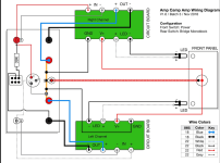
Hello everyone! I'm building two ACA monoblocks with a friend. The goal is to have a single-ended input (white/black RCA jack per build guide), XLR as standard, AND balanced mono TRS spliced into the XLR on the back panel (per his request, I've informed him I don't think it will work as he intends but he is insistent, and I am curious).
To accomplish this, I've done three things:
1. REMOVED the red RCA jack, replacing it with a 3-position junction block.
2. REMOVED both red binding posts, as the amplifier will never function in stereo operation. Instead, a ground bus links all previous connections together (I replaced one [1] black binding post with a red binding post in my modified wiring diagram)
3. ADDED a TRS jack with the pin-out in the bottom right of the diagram. T=> pin 2 ; R=> pin 3; S=> pin 1
However, I have a problem with my Schematic; what happens with the RED (now deleted) RCA shield wire coming from the negative input of that amplifier board? I have made a big green box around this wire in my Schematic, with Jeopardy-style questions above it
Do we:
A. Split the shield wire of our single-ended input to both amplifier boards
B. Connect the negative input of one board to the power supply ground
C. Ignore it. Pretend it never happened, never install one. And move on
D. Something Else?
Please point out any flaws you see or questions you have! All help and advice is appreciated!
(Following v1.6 Schematic as I prefer two-position rear switch DOWN=XLR; UP=SINGLE-ENDED MONO. Open to any recommendations on switches)
Purple circles represent deleted connectors, instead junctions are used.
I'm building two ACA monoblocks with a friend. The goal is to have a single-ended input (white/black RCA jack per build guide), XLR as standard, AND balanced mono TRS spliced into the XLR on the back panel (per his request, I've informed him I don't think it will work as he intends but he is insistent, and I am curious).To accomplish this, I've done three things:
1. REMOVED the red RCA jack, replacing it with a 3-position junction block.
2. REMOVED both red binding posts, as the amplifier will never function in stereo operation. Instead, a ground bus links all previous connections together (I replaced one [1] black binding post with a red binding post in my modified wiring diagram)
3. ADDED a TRS jack with the pin-out in the bottom right of the diagram. T=> pin 2 ; R=> pin 3; S=> pin 1
However, I have a problem with my Schematic; what happens with the RED (now deleted) RCA shield wire coming from the negative input of that amplifier board? I have made a big green box around this wire in my Schematic, with Jeopardy-style questions above it
Do we:
A. Split the shield wire of our single-ended input to both amplifier boards
B. Connect the negative input of one board to the power supply ground
C. Ignore it. Pretend it never happened, never install one. And move on
D. Something Else?
Please point out any flaws you see or questions you have! All help and advice is appreciated!
(Following v1.6 Schematic as I prefer two-position rear switch DOWN=XLR; UP=SINGLE-ENDED MONO. Open to any recommendations on switches)
Purple circles represent deleted connectors, instead junctions are used.
Attachments

At circuit board, note the (+ out) and G (your wire in question) are parallel. If you measure the dangling wire right now to your ground bus. You’ll find it is already connected to the ground bus. But keep the pair twisted to your new connection: and connect the lead you took off to the bus as close to the new connection as you can to aid with noise cancellation.
Perhaps a simpler way to get where you seem to be going with this would be to make an Adapter cable for TRS to XLR when you want to use the balanced mode.
And an XLR that shorts pin 2 and 3 together when you want to use the single end mode.
Perhaps a simpler way to get where you seem to be going with this would be to make an Adapter cable for TRS to XLR when you want to use the balanced mode.
And an XLR that shorts pin 2 and 3 together when you want to use the single end mode.
Attachments
That is great insight, taught me to look at the dang board!🤦🏼♂️ You're definitely right about simplifying to XLR- but this amplifier is for a friend, who made the decision to go this route for personal preference. Your time is much appreciated 😊 I'll post photos once the project is complete!
Totally up to you and your friend, you may have already considered this, and ... you didn't ask... so... apologies.
I'd consider the 'relative' phase between your RCA input and your XLR/TRS input related to the output if you don't change speaker cabling between the two. It looks like they would not be the same. May not matter to you at all.
Since you don't have a 'GND referenced' output in any situation, after deciding on the above, I'd consider which binding post should be red or black. May not matter to you at all.
Again, you didn't ask, but if I were doing something similar, I'd match the relative phase of the outputs regardless of input to the same binding posts. That way I wouldn't need to swap speaker cables to maintain the same relative phase when switching from the RCA input to the XLR / TRS. I'd also go with the red binding post aligned with the signal in-phase with the input, and the black binding post aligned with the inverted phase signal.
It will work just as you've diagramed, but ... it's a matter of preference. Just sharing my preference. Thinking about the inverted phases makes my head hurt... so, if I've got this mixed up, my apologies.
Soldering is awful in post #11943 and similar ones. Guys, please learn how to solder before you start assembling DIY kits.
https://www.diyaudio.com/community/threads/amp-camp-amp-aca.215392/post-7509245
https://www.diyaudio.com/community/threads/amp-camp-amp-aca.215392/post-7509245
Yes, soldering is not great with some people but so what?
What counts is the end result, the project works and provides satisfaction, pleasure, elation.
They are learning and everyone is entitled to make their own mistakes.
The rest of us are here to notice their mistakes and encourage them to do better, not to put them down and proclaim our imaginary superiority.
You can offer suggestions how to improve their soldering skills instead.
Let me see your soldering work first.
I bet I'll find a few problems with it but who cares if it works at the end.
Please keep your unpleasant outbursts to yourself.
Let me see your soldering work first
Frankly, I do not have an archive of soldering jobs, so I can only dig in my stock and make a photo of some old prototype

My advice was quite sincere - without reliable assembly and soldering you may expect any kind of “unexplainable” failures. I am saying that as someone who spent 40+ years in electrical engineering and electronic design and who has assembled, soldered and tested about 4000 PCB boards. Just an advice.
- Home
- Amplifiers
- Pass Labs
- Amp Camp Amp - ACA