Never mind. I found this. Thanks agdr for already answering my question for someone else!
Those are the voltage regulators, U5 and U6, that are backwards not the mosfets. The mosfets look OK from the photo. C6 and C7 look like MLCC rather than film but it shouldn't matter.
The pinouts are different on those regulators. The positive regulator, MC7812, may have survived since input and output were swapped. Maybe not so much for the negative regulator, MC7912, because that would swap ground the output. If it were me I would replace both with new chips. LM7812 and LM7912 would work just fine.
The regulators will come right out if you take a piece of copper desolder braid a half inch long or so and place it across all 3 pins on the back of the PCB, then heat the braid with your soldering iron so all 3 pins get hot at once. Support the PCB so the part with the regs has nothing underneath so the regs can fall out. The holes in the PCB are big enough that gravity will cause them to drop right out onto the ground once the solder on all 3 pins melts.Actually kind of fun, I've done it a few times, lol.
Check that the regulators were in the right spots, too, once you get them out. The negative MC7912 is the one closest to the edge of the PCB.
Another issue is the output chips in your photo, the two in the middle, are the low power TLE2062CP option on RocketScientist's BOM rather than the standard higher current NJM4556s. The TLEs are fine, but can't drive nearly as much current to the headphones as the NJMs can. Plus have slightly more distortion, although it probably isn't audible. The details are in RocketScientist's blog here NwAvGuy: O2 Details
Mayday! A long strand of solder strung out from a spindle was laying across my worktable. While the o2 plugged in and was being tested, it brushed over the top of this solder cable. Much to my dismay and surprise, it sparked and hissed a little underneath.
Luckily, I was only on the testing step where no op-amps were in, U1-U4 not inserted. However, I am unsure what I fried, because the voltage is definitely off, 18 V.
RocketScientist's guide leads me to believe either Q1, Q2 or both were damaged. Now, can I replace these with any N and P MOSFETS as long as they are minimally 24V vds? Do they need to be from the same series and brand? Any thoughts? Thanks!
If the regulators are working correctly, there shouldn't be >12V referenced to ground in the power management or signal gain sections of the O2.
You hit the nail on the head. (By the way, I like the creative username, sofaspud!) This is exactly the problem that I am facing. When I got to the section "Install Only U2 Next", I was getting ~0.1 V on pin 4 and ~14V magnitude on pin 8. Then and there, I knew it was most definitely a case of a couple toasted Q1s and Q2s.
One heads-up: I will be busy for the next week and a half. However, I have plenty of Fairchild Semiconductor samples on delivery, 10 of each. If anything should go wrong with these electrostatically challenged chips, I will have an entire arsenal of them at the ready should one fall out of line again or if another assembling error fries them. At that point when I return, I will keep you all updated with pictures so you can share in the joy of my final success.
Last edited:
I am looking into alternatives to Q1 and Q2 since I may or may not be able to get the samples from Fairchild. Note that I do not want to ruin the O2's benchmark performance. Are there any different N or P Ch MOSFETs that fit the specifications of Vgs > 24V Vds > 25V Rds < 0.5 ohms IPAK GDS? As someone once asked, is there any concern about them being imbalanced to each other? I am willing to seek alternatives from TI, On Semi, Vishay, and others.
I am looking into alternatives to Q1 and Q2 since I may or may not be able to get the samples from Fairchild. Note that I do not want to ruin the O2's benchmark performance. Are there any different N or P Ch MOSFETs that fit the specifications of Vgs > 24V Vds > 25V Rds < 0.5 ohms IPAK GDS? As someone once asked, is there any concern about them being imbalanced to each other? I am willing to seek alternatives from TI, On Semi, Vishay, and others.
Is there a rule against bumping? I am bumping now, but, if so, I will never do it again.
Is there a rule against bumping? I am bumping now, but, if so, I will never do it again.
You can ask for help from agdr, he is one of the few experts on O2 mods (and circuit designer for O2 desktop amp) who can guide you.
...The gain button, what does it do?
The gain switch gives 2 options-
High-gain for high impedance/low sensitivity cans/ weak input sources like mp3 player/ipod e.t.c.
Low gain(recommended) for low impedance/high sensitivity cans/ strong input sources like ODAC/CD player line out
further reading NwAvGuy: O2 Details
I am looking into alternatives to Q1 and Q2 since I may or may not be able to get the samples from Fairchild.
I wouldn't have any suggestions there, but those mosfets are around $0.80 at Mouser. Hard to beat that.
I wouldn't have any suggestions there, but those mosfets are around $0.80 at Mouser. Hard to beat that.
OK. Thank you! The ever so slightly pricey part about the shipping, not the product itself, is what bothers me.
Quote:
Originally Posted by Vigo View Post
...The gain button, what does it do?
The gain switch gives 2 options-
High-gain for high impedance/low sensitivity cans/ weak input sources like mp3 player/ipod e.t.c.
Low gain(recommended) for low impedance/high sensitivity cans/ strong input sources like ODAC/CD player line out
further reading NwAvGuy: O2 Details
Thank you availlyrics, good explanation
OK. Thank you! The ever so slightly pricey part about the shipping, not the product itself, is what bothers me.
Try living in europe, anything you buy costs at least €20 to ship, or if you spend over €60 you get free shipping... so before you know it you have bought €40 worth of crap you didnt need just to get that one part you did. Damn you mouser
I am a first class cheapskate--or would that be third class, saddled camel through the Arabian desert, canoe braving the ocean waters, all in the name of that last cent, no better than Scoorge McDuck, cheapskate?
I am going to order from Digikey using the free shipping via check or money order trick. Since it's been a while, it took me some time to remember that Digikey had that special clause in place (see #6 http://dkc1.digikey.com/us/en/mkt/Terms.html ). Just pay about half a buck for postage, enclose your check or money order and--presto!--free shipping.
UPDATE: After further explanation to the Fairchild representative, I now have the parts on delivery, five each of the stock MOSFETs. No Digikey for now. Luckily, I did not strike the ink to the check yet!
Last edited:
Maybe thats right, 9v x2 = 18v. Have you tested these points,
An externally hosted image should be here but it was not working when we last tested it.
Last edited:
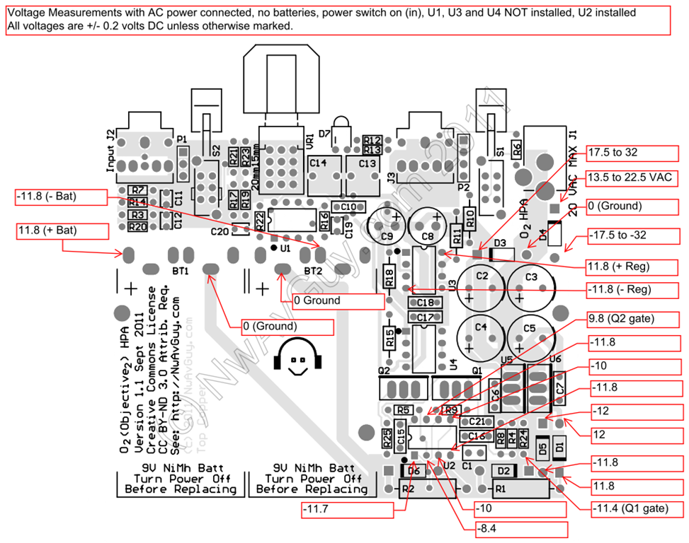
Take voltage measurements along the power supply path - AC input first, then ground referenced DC across the filter caps, regulator inputs, each side of D1 & D5. This can be done with the unit off and verifies the power supply operation.
If that checks out OK, the unit can be switched on and the DC distribution to the rest of the circuit can be checked.
If that checks out OK, the unit can be switched on and the DC distribution to the rest of the circuit can be checked.
Maybe thats right, 9v x2 = 18v. Have you tested these points,
An externally hosted image should be here but it was not working when we last tested it.
Thank you everyone so far! Using this as a blueprint, and measuring as specified, ground (BT1-) to each point, but without U2 installed and the device "off":
BT1+: 17.32 V
BT2-: -0.01V
D3 (left/right): 18.06 V/ 0 V
D4 (bottom): -18.13 V
U4 (P4/P8): .67/.16
U2 (all pins): 0.01-0.02 V
D5 (top/bottom): Starts around 3.5 V, lowering/
D1 (top/bottom): 17.34 V/17.34 V
For reference, I am using all the recommended parts as listed in the BOM. Previous to voltage testing, all resistor values had been tested and verified.
Last edited:
- Home
- Amplifiers
- Headphone Systems
- The Objective2 (O2) Headphone Amp DIY Project