Hello TNT,Nice! There are many circuits now for power stabilisation - why just TPS7A...? Not that there is something bad with it - just curious!
//
Why not ?
The TPS7A87 is very low noise and allow two regulated outputs in small package and also is cheap and easy to find.
Nice job! Take care about connecting the clock oscillator directly on the analog 3.3va power, as it rather belongs to the epld. Check also the spdif outputs in this regard.
Otherwise I like it very much! Maybe you could connect sdi of the ad's to the epld as well (if you have any spare pins), later on it could add some flexibility reaching the adc internals.
Regards
Attila
Hello Atilla,
Don't worry, all power rail well separated: 3.3VA is digital supply for ADC and clock I/O path. The 3.3V is only for CPLD and isolators.
About the SDI, i can be only use to read-back average setting so i don't find this very useful (no ?). I keep this in mind anyway...
Well,
all on your Analog & ADC board has the same ground, as
. Input
. Relays
. Digital
. ADC
Consider to group & split the required grounds in different groups ... while a simple relays current would/may induce ugly current within the input ground..
May also consider multiple PCB ground layers ..
At the end symmetric/asymmetric input measurements will tell you how good the PCB implementation is.
just my 2 cents
Hp
Hello Hp,
I disagree (sorry
") )
)In most case ground splitting is bad idea, and can cause major EMC issue.
Using massive uncutted single ground plane is generally the best.
Of course, a right parts implantation is crucial to avoid ground current noise created by
fast parts (logic devices) and contaminate analog sensitive path.
(even LT recommend this in their datasheet or as in their EVM).
Hi Frex,
A couple of comments could be that:
- it looks as if the CNV signal passes through some ICs before reaching the CNV input. Although I realize that SAR converters are less prone to phase noise than delta-sigma converters I personally would do my best to ensure that this signal is as clean as possible (low phase noise ICs etc.). Andrea Mori's thread on the well-tempered clock has some info on this.
- Second I notice that you use regulators that are just reasonably low-noise. Might it be an idea to use something like e.g. LT3042? In my experience the LTC2380 is quite sensitive to the noise input to its various PSU pins.
- The layout made by LT themselves has some validity. Just by moving and slightly re-arranging capacitors around the Vdd and IOVdd pins to reflect LTs layout (spacing of the Vdd & IOVdd ground) I got a distortion reduction on the order of -15 dBs. I reckon what happens here is that ground return paths from the digital side may influence the ground potential on the Vdd pin.
Cheers,
Jesper
Hello Jesper,
For lowest possible jitter, the CNV (sampling clock signal) is synchronized to the main low phase noise oscillator
by using the flip-flop before to be send to the ADC CNV input. SO you don't take care about about jitter on CPLD CNV output.
The 7A87 output noise is already very low, but maybe i could try to allow dual footprints implantation.
Note that the LT3042 is also much expensive.
About supply pins decoupling capacitors placement i agree, there is essential to place them
at the right place to get best performance. I think to follow carefully LT EVM design that is work great.
You seem to have already made yourself a design with this ADC, can you tell us more about this ?
Thanks to all for comments.
Frex
Hi Frex,
Well, we have been three people doing this work - two programmers (FPGA/"other") and then myself doing the hardware design. The main aim has been to create a system capable of sampling at 1.536 MHz at the best possible sound quality (to be used for recordings). We have succeeded in sampling at 1.536 MHz and transferring these data into the PC, however, currently this work is a bit on hold mainly (but not only) because there has been a "transmission" bottle neck somewhere in the transmission from the FPGA board to the PC ... Thus, we can transfer one channel of 1.536 MHz data but not stably more than that. And currently with a maximum transfer time of about 10 mins.
That said I think the LTC2380 indeed has a potential. 2H distortion levels has been around - 120 dBs (12 kHz sine; lower distortion for higher harmonics) and I reckon the main reason for this has been that I have used a couple of AD797s with no distortion adjustment as the front end. Their THD level is around - 120 dBs when not distortion adjusted.
My experience with trying different decouplings on the LT2380 has been that what LT suggests themselves leads to the lowest noise levels - also frequency wise - on the supplies. Thus basically using 47 uF in combination with 100 nF leads to less overall noise on the Vref pin than using e.g. 0.33uF or 0.47 uF in combination with 22uF,100uF, 68 uF etc.
Yes, I know. Yet, while I personally am not interested in a 192 kHz recording system, I reckon that if what you do is to be used for recording purposes then using an LT3042 may be well worth the slightly higher overall price. But, being honest here - I haven't listened to the LT3042 nor the regulator you suggest ... But I note that the LT3042 has gained a good reputation.
Cheers,
Jesper
You seem to have already made yourself a design with this ADC, can you tell us more about this ?
Well, we have been three people doing this work - two programmers (FPGA/"other") and then myself doing the hardware design. The main aim has been to create a system capable of sampling at 1.536 MHz at the best possible sound quality (to be used for recordings). We have succeeded in sampling at 1.536 MHz and transferring these data into the PC, however, currently this work is a bit on hold mainly (but not only) because there has been a "transmission" bottle neck somewhere in the transmission from the FPGA board to the PC ... Thus, we can transfer one channel of 1.536 MHz data but not stably more than that. And currently with a maximum transfer time of about 10 mins.
That said I think the LTC2380 indeed has a potential. 2H distortion levels has been around - 120 dBs (12 kHz sine; lower distortion for higher harmonics) and I reckon the main reason for this has been that I have used a couple of AD797s with no distortion adjustment as the front end. Their THD level is around - 120 dBs when not distortion adjusted.
My experience with trying different decouplings on the LT2380 has been that what LT suggests themselves leads to the lowest noise levels - also frequency wise - on the supplies. Thus basically using 47 uF in combination with 100 nF leads to less overall noise on the Vref pin than using e.g. 0.33uF or 0.47 uF in combination with 22uF,100uF, 68 uF etc.
Note that the LT3042 is also much expensive.
Yes, I know. Yet, while I personally am not interested in a 192 kHz recording system, I reckon that if what you do is to be used for recording purposes then using an LT3042 may be well worth the slightly higher overall price. But, being honest here - I haven't listened to the LT3042 nor the regulator you suggest ... But I note that the LT3042 has gained a good reputation.
Cheers,
Jesper
We have succeeded in sampling at 1.536 MHz and transferring these data into the PC
Did you used USB based transmission (XMOS) or else gear?
Thus, we can transfer one channel of 1.536 MHz data but not stably more than that. And currently with a maximum transfer time of about 10 mins.
Does this means after 10 minutes, getting transmission errors or?
My experience with trying different decoupling on the LT2380
As ARDA AT2101 AN 1: Using an active buffer/drive, the THD+N was below 200Hz better performing..
Hp
Hi HpW,
We used a digilent Zedboard with ethernet transmission and a custom "written" "receiver software" at the PC end. It should be capable of sustaining a much higher transfer rate but for some reason it cannot manage more than about 70 Mbps.
Yes - and often the transmission stops.
I am not quite sure what you mean here (BTW: ARDA 1201 I guess?). I reckon that active buffering may be a solution to some challenges but it also e.g. adds complexity ... I prefer not to use this kind of decoupling.
Hope this answers your questions - Cheers,
Jesper
Did you used USB based transmission (XMOS) or else gear?
We used a digilent Zedboard with ethernet transmission and a custom "written" "receiver software" at the PC end. It should be capable of sustaining a much higher transfer rate but for some reason it cannot manage more than about 70 Mbps.
Does this means after 10 minutes, getting transmission errors or?
Yes - and often the transmission stops.
As ARDA AT2101 AN 1: Using an active buffer/drive, the THD+N was below 200Hz better performing..
I am not quite sure what you mean here (BTW: ARDA 1201 I guess?). I reckon that active buffering may be a solution to some challenges but it also e.g. adds complexity ... I prefer not to use this kind of decoupling.
Hope this answers your questions - Cheers,
Jesper
What is the size of your ethernet frames? windows throttles interrupts to retain multitasking usability, so if you use very small frames = many interrupts, you will get interrupt-throttled. This is the reason why ethercat with its small packets is very bandwidth limited.
If you are using small frames, then enlarge them with more data in each frame.
If you are using small frames, then enlarge them with more data in each frame.
What is the size of your ethernet frames? windows throttles interrupts to retain multitasking usability, so if you use very small frames = many interrupts, you will get interrupt-throttled. This is the reason why ethercat with its small packets is very bandwidth limited.
If you are using small frames, then enlarge them with more data in each frame.
May we should have a separated thread, while not to ..... the current thread!
Jumbo frames is the key! But requires HW who is cable of.
Guidance on the use of jumbo frames | Answer | NETGEAR Support
May look also on AVB/Dante how they deal with this.
hp
I wonder how this thread managed to stay unseen here for so long. 
Good work!
I'm just doing a similar ADC. Originally it was intended to be just a quickie
because my 89441A analyzer has such a bad 1/f noise.
Since I use BeagleBone Blacks for other things, the idea was to use its
48MBit/sec SPI interface to read out the ADC. I settled on the LTc2500-32.
The 2500 needs a 100 MHz SPI clock at full sample rate, so that gave the
oscillator frequency the 1 MHz sample rate was derived from. When a
conversion is started, the LTC2500 wants to be left alone for 650 nsec
for best analog performance, so the 32 bits have to be saved in 350 nsec
before the next conversion starts.
Since I'm interested in 1/f, I was willing to accept the limitations of the BBB's
48 MHz SPI. I lost a lot of time on that and could not get the SPI interface to
work under the BBB's Debian Linux.
I noted that the Xilinx Coolrunner CPLD that generates the sample clock had
just enough resources (64 flipflops total) to implement a 32 bit SPI receiver.
The BBB has a 1 GHz ARM CPU with hardware floating point and two additional
200 MHz RISC I/O processors called PRUs. The PRUs need 5 nsec/instruction
and don't use pipelining, so execution is highly time predictable, you can set
port bits with 5 nsec resolution. The I/O processors have nothing to do with the
Linux system if you want that, but there is a C compiler etc on the BBB that can
translate the PRU programs and load & start them. The 2 PRUs and the master
ARM CPU can talk together via a shared RAM.
Since the BBB tries to be everybody's darling, use of I/O pins is quite complicated;
a lot of the work is to sort out how to get rid of the graphics display and its drivers
that are installed by default. I found out that PRU1 can access an 8 bit field on
the P8/P9 plugs and some more single bits. So I decided to read in the SPI data
in 4 bytes for each sample.
Timing is fast enough that I could read out 3 ADCs at full speed, so I could
compute the 3-cornered hat. ( Cross correlation 1-2, 2-3, 3-1 so you can
attribute signal & noise to the 3 inputs.)
The PRU receives a data-ready signal from the CPLD and then fetches the
4 bytes and merges them to 32 bit samples again. The samples are deposited into
a 2*1Ksample ping-pong buffer. When 1Ksample is complete, the ARM fetches
it while the PRU fills the other buffer.
That also fixes easily the transition from the hardware buffer to the ARM's virtual
memory land where RAM is plenty. The ARM could then compute FFTs in its
NEON floating point unit, do averaging etc. It could also run a web server to
display the results, much like the STEMLAB in the Red Pitaya.
I already could install the fftw library. (fastest FFT in the west)
I decided for the first step to imitate the 89441A's remote control interface and
simply pass the data on via LAN. I can simply open port 5025 on 192.168.178.111
on my laptop and read/write GPIB/IEEE488/SCPI-like commands.
The ARM runs a server for that and it was not very hard to do. The network i/f
under Debian is maybe 3 pages of C, once one has understood the principle.
All software work can be done on the Linux system, the compilers, editors etc
are all included in the Debian distribution. You can simply ssh into it from your
laptop and have shell access.
Hardware-wise there is not too much to it. There is a stamp-sized board that
is the home for the CPLD and another stamp for the LTC2500-32. The second
stamp has also 2 LT3042 for the analog voltages, a LT6655 reference and the
differential ADC driver as proposed in the 2500 data sheet. The is also a -3V
regulator for the ADC driver. I have not yet made up my mind what comes
in front of the ADC driver. I'm into measuring stuff and not into audio recording.
regards, Gerhard
Attachments
Hello all,
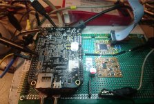
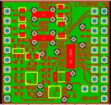
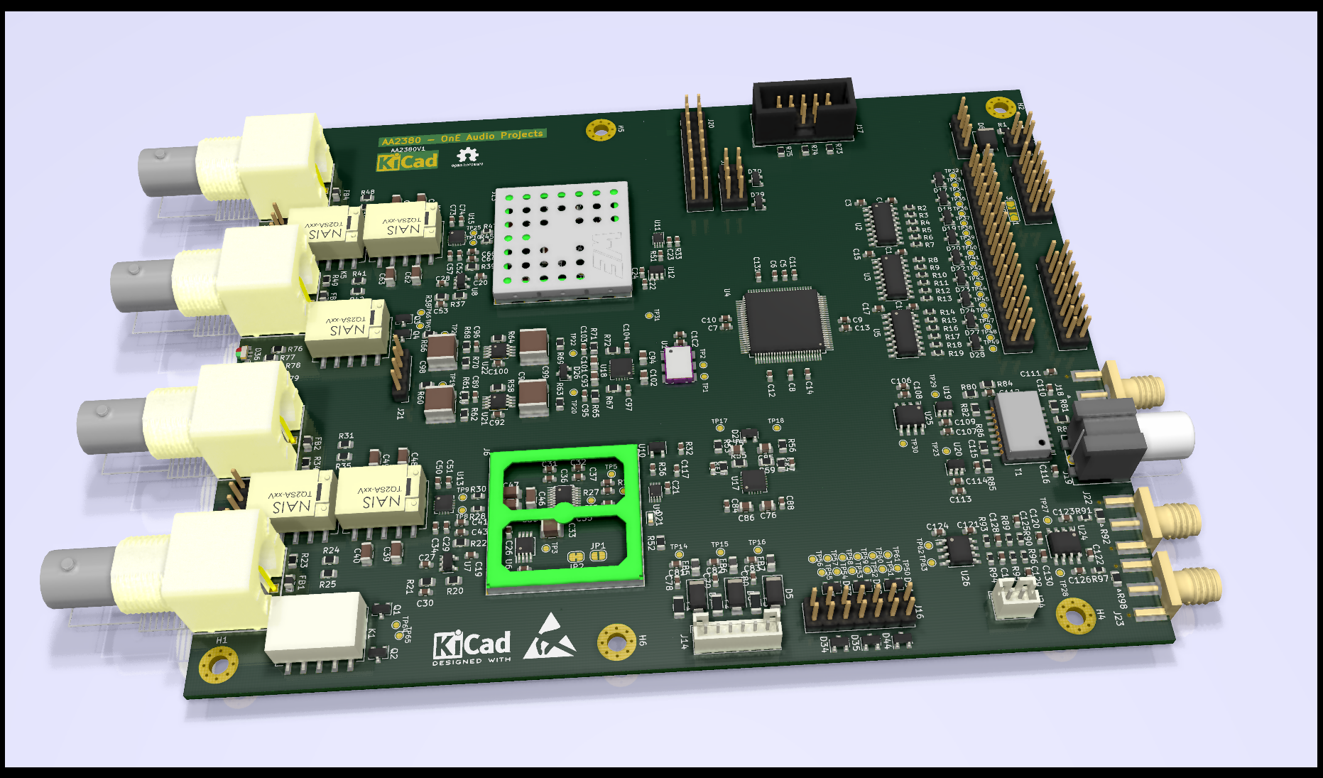
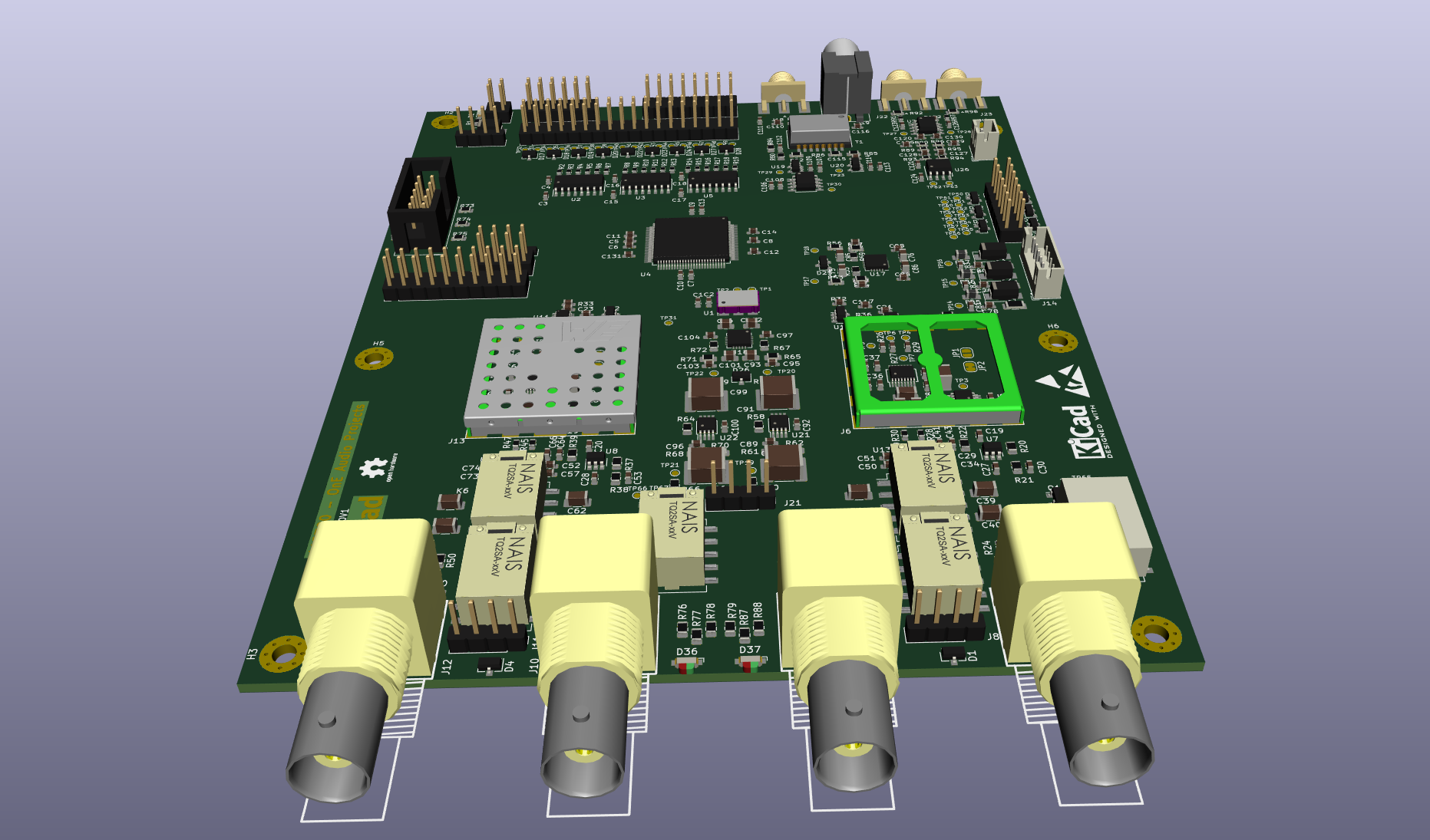
Just to show the actual project progress, some pictures of the (uncompleted)
parts placement on PCB of the AA2380 PCB.
I will post also soon an updated schematics.
That's on the right way !
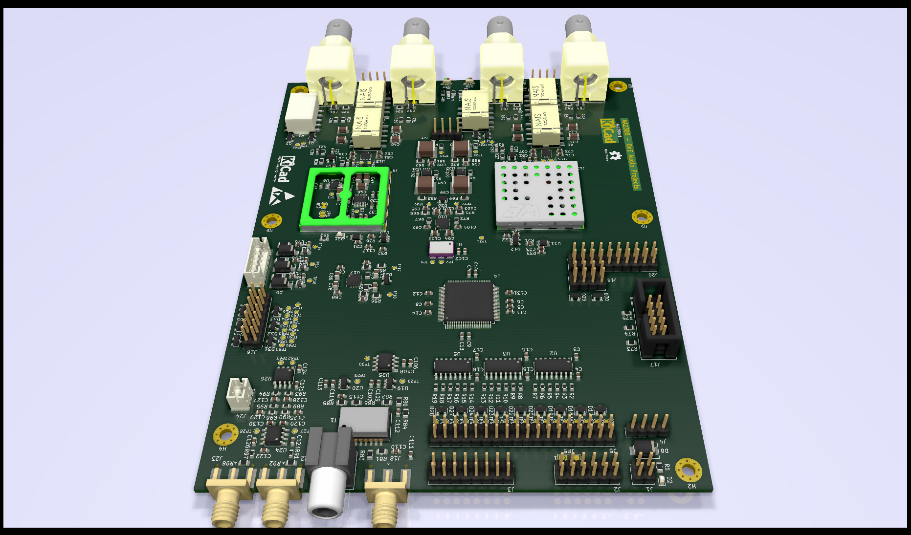
Frex
Nice !
What size are your SMD resistor and smallest smd parts ? 0805, 0603 or smaller ?. Hand soldering with parts smaller than 0805 is not easy with an hot air gun...and not everybody got an oven.
Chris
Hello Chris,
I tried to use not too tiny parts, so it's a mix of 805 and 603 sizes.
Small sizes are much convenient for closer decoupling, and so they are not so hard to solder.
But i Agree you will probably need a magnifying lens close to you !
Note that for now i personally make only hand soldering.
I don't have an oven, but i really think about getting one...
(I think some 0.5mm pitch IC are harder to solder properly).
Frex
Hi Guys, wonderful work Frex.
I hand solder 0.5mm pitch and 0805,0603, but you need a steady hand, a good magnifier, a stereo microscope is the best if you can justify the expense, I can not. The DFN/QFN is a PITA, you have to make a special padstack, with a bigger SMask opening to get the tip onto, if you are going to hand solder it.
Found that no-clean glow core eutectic solder to be my choice, lead free is a PITA, our hobbies do not need to be lead free, just like aero-space apps = exempt.
I like your RF covers, I was using them in a RF design.
If you are going to build a few, then the stencil, paste, reflow oven is a nice to have but for a few proto's, it is not worth it unless it is a very populated, complex design, BGA it is essential. Placing fine pitch parts in paste is hard to do by hand. I once designed a pcb with a 1152 pin Xilinx a bunch of IDT dual port SRAM, 10G Intel SerDes on 0.4mm BGA's, impossible by hand, Sanmina/SCI pls.
Last edited:
Hello Frex,
I saw here SAR ADC for high performance audio ADC project [LTC2380-24]
you have been testing USB-I2S PCB from SDR-Widget.
Right now i am testing the same board but work only in UAC1 mode, not UAC2 even with ASIO drivers.
What drivers did you use for Win 7 64bit ?
Regards!
I saw here SAR ADC for high performance audio ADC project [LTC2380-24]
you have been testing USB-I2S PCB from SDR-Widget.
Right now i am testing the same board but work only in UAC1 mode, not UAC2 even with ASIO drivers.
What drivers did you use for Win 7 64bit ?
Regards!
Hello all,
There is some news about the project.
For the first release of the project, i decided to start a new clean project.
You can access it here : OSVA - Open Source Versatile Analyzer.
Regards
Frex
There is some news about the project.
For the first release of the project, i decided to start a new clean project.
You can access it here : OSVA - Open Source Versatile Analyzer.
Regards
Frex
Hi,I don't know if the performance is better or worse, but you could consider taking the clock in and converting it to LVDS for distribution and isolating it with ADN4650. There is no phase noise vs frequency graph though, but the HF jitter specs look ok. Probably unnecessary but you can then distribute the clock as LVDS internally.
Analog Devices's LVDS isolator is explicitly better than single end isolator!
My DIY DAC is universal board base (ADN4654 is mounted on half pitch surface mount universal board), then I used Molex TwinMax twin axial cable.
It improved sound orientation.
Temp-Flex TwinMax: Twin-Axial Cables - Molex | DigiKey
TwinMax is semi-ridgit like hard and high temperature resistive cable.
If you couldn't use impedance controled PCB, I recommend this cable.
I bought 10 feet of TwinMax at Digikey, but they send 10 unit of 1 feet cable!
If you want longer cable, it will be better to place an order for 25 feet.
Edit: fixed Digikey.jp to Digikey.com
Last edited:
- Status
- This old topic is closed. If you want to reopen this topic, contact a moderator using the "Report Post" button.
- Home
- Design & Build
- Equipment & Tools
- SAR ADC for high performance audio ADC project [LTC2380-24]